
NANO EXPRESS Open Access
Characterization of silicon heterojunctions for
solar cells
Jean-Paul Kleider
1*
, Jose Alvarez
1
, Alexander Vitalievitch Ankudinov
2
, Alexander Sergeevitch Gudovskikh
3
,
Ekaterina Vladimirovna Gushchina
2
, Martin Labrune
4,5
, Olga Alexandrovna Maslova
1,3
, Wilfried Favre
1
,
Marie-Estelle Gueunier-Farret
1
, Pere Roca i Cabarrocas
4
, Eugene Ivanovitch Terukov
2
Abstract
Conductive-probe atomic force microscopy (CP-AFM) measurements reveal the existence of a conductive channel
at the interface between p-type hydrogenated amorphous silicon (a-Si:H) and n-type crystalline silicon (c-Si) as well
as at the interface between n-type a-Si:H and p-type c-Si. This is in good agreement with planar conductance
measurements that show a large interface conductance. It is demonstrated that these features are related to the
existence of a strong inversion layer of holes at the c-Si surface of (p)a-Si:H/(n)c-Si structures, and to a strong
inversion layer of electrons at the c-Si surface of (n)a-Si:H/(p)c-Si heterojunctions. These are intimately related to
the band offsets, which allows us to determine these parameters with good precision.
Introduction
In the field of silicon solar cells, recent progress has
been achieved in two directions: silicon heterojunctions
and silicon nanowires. These two topics are briefly
addressed here and we show some new characterization
results that use conductive-probe atomic force micro-
scopy (CP-AFM) measurements.
Silicon heterojunctions are formed between crystalline
silicon (c-Si) and hydrogenated amorphous silicon (a-Si:
H). Solar cell efficiencies of up to 23% have been demon-
strated on high quality n-type c-Si wafers with layers of
p-type a-Si:H deposited at the front (as the emitter) and
n-type a-Si:H deposited at the back (as the back surface
field), respectively [1]. Since transport properties are quite
poor in a-Si:H due to the large amount of defects and
band gap states and low carrier mobilities, the doped a-Si:
H layers are used to form the junctions, but their thickness
has to be kept very low. The front a-Si:H layer has to be
very thin in order to minimize absorption of incoming
photons and to privilege absorption in c-Si. One key fea-
ture of the Si heterojunctions is the very good passivation
property of the c-Si surface by a-Si:H. This is even
improved by inserting a thin undoped a-Si:H layer
(so-called “intrinsic”layer, which leads to the “HIT”-
heterojunction with intrinsic thin layer denomination [2]).
This limits interface recombination and leads to very high
open circuit voltages [3]. Band offsets between a-Si:H and
c-Si also play a crucial role because they determine the
band bending, which influences the carrier collection. We
here demonstrate the existence of a conduction channel
along both the (n)a-Si:H/(p)c-Si and the (p)a-Si:H/(n)
c-Si interfaces from direct CP-AFM measurements per-
formed on cleaved sections of solar cells. We show from
additional planar conductance measurements and simula-
tions that these are related to strong inversion regions
at the interfaces. From the temperature dependence,
we determine the values of band offsets.
Experimental details
Solar cell structure
A typical solar cell structure based on a-Si:H/c-Si het-
erojunctions formed with n-type c-Si is presented in
Figure 1. A similar structure stands for p-type c-Si,
replacing the n-type a-Si:H by p-type a-Si:H and vice
versa. For n-type c-Si, we used Float Zone, n-type c-Si
wafers, 〈100〉oriented, with resistivity: r=1-5Ωcm,
and thickness: W= 300 μm. For the p-type c-Si,
we used Czochralski (CZ) c-Si wafers, 〈100〉oriented,
with resistivity: r= 14-22 Ωcm, and thickness: W=
300 μm. We used indium tin oxide (ITO) as the front
* Correspondence: jean-paul.kleider@lgep.supelec.fr
1
Laboratoire de Génie Electrique de Paris, CNRS UMR 8507, SUPELEC, Univ
P-Sud, UPMC Univ Paris 6, 11 rue Joliot-Curie, Plateau de Moulon,
91192 Gif-sur-Yvette Cedex, France.
Full list of author information is available at the end of the article
Kleider et al.Nanoscale Research Letters 2011, 6:152
http://www.nanoscalereslett.com/content/6/1/152
© 2011 Kleider et al; licensee Springer. This is an Open Access article distributed under the terms of the Creative Commons Attribution
License (http://creativecommons.org/licenses/by/2.0), which permits unrestricted use, distribution, and reproduction in any medium,
provided the original work is properly cited.
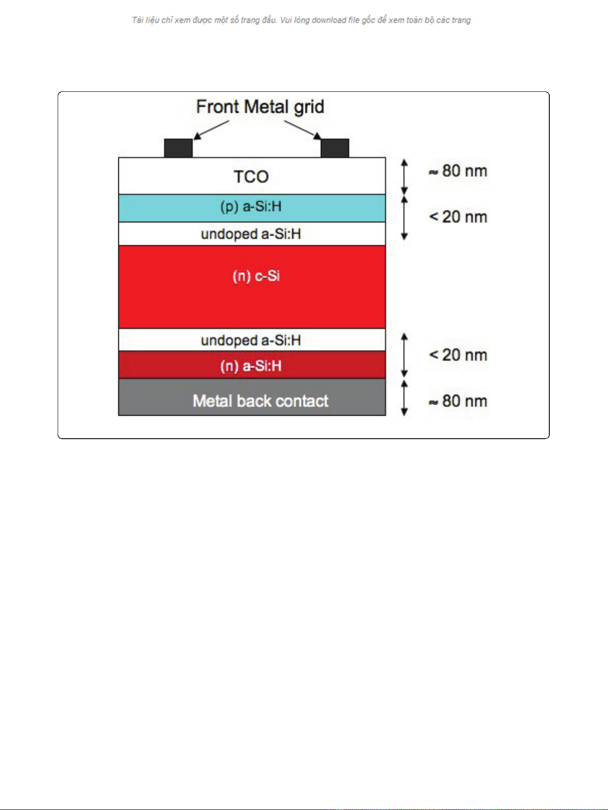
transparent conductive oxide (TCO), and aluminum as
the back metal contact. The a-Si:H layers were depos-
ited at Ecole Polytechnique in a radio frequency (13.56
MHz) plasma-enhanced chemical vapor deposition
(PECVD) reactor at a substrate temperature of 200°C.
Spectroscopic ellipsometry measurements and modeling
were used to check that the deposited silicon thin layers
were truly amorphous, and that no epitaxial growth
occurred on the c-Si substrate.
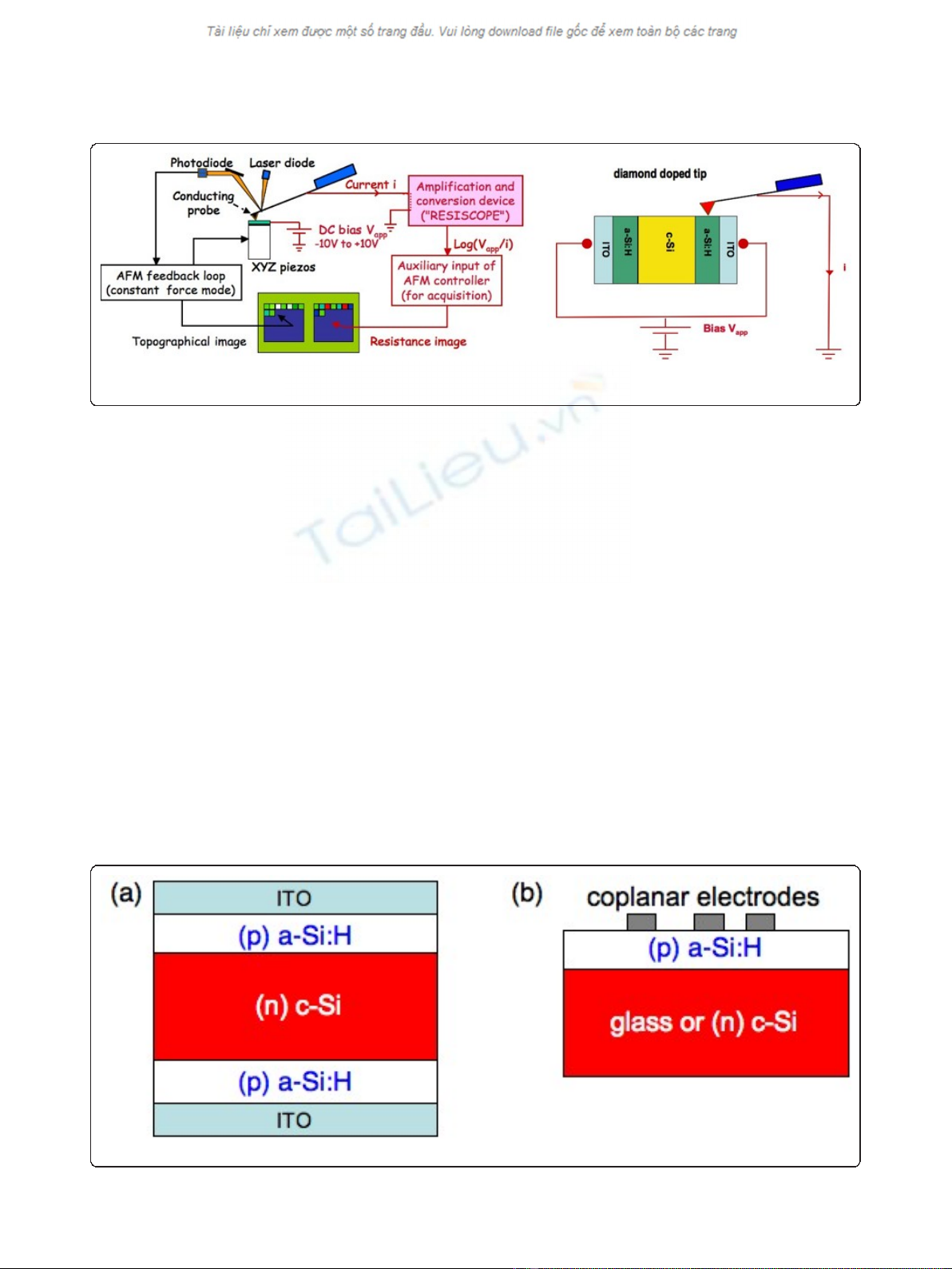
CP-AFM
CP-AFM measurements were carried out using two dif-
ferent setups (i) in Ioffe Physical-technical Institute
(NT-MDT Ntegra Aura) and (ii) in Laboratoire de
Génie Électrique de Paris (Digital Instruments Nano-
scope IIIa Multimode AFM with the RESISCOPE exten-
sion [4]). These setups allow one to apply a stable DC
bias voltage to the device and to measure the resulting
current flowing through the tip as the sample surface is
scanned in contact mode. Schematic AFM setup is
shown in Figure 2. In both measurements diamond-
coated conductive probes made of silicon were used, the
contact interaction force being in the range 100-500 nN.
With the help of this technique one can simultaneously
examine on the sample cleavages the surface topography
and conductive properties of the layers constituting the
solar cells. Note that, due to different softwares, the first
setup provides images with current values (current flow-
ing through the tip), while the second one provides
resistance values, the resistance being defined as the
ratio of the applied voltage to the measured current.
For these CP-AFM measurements, the normal solar
cell structure was replaced by a simpler symmetric con-
figuration, see Figure 3a, where the same a-Si:H layer
was deposited on both sides of the c-Si wafer. Then
ITO electrodes were deposited on top of both sides of
the wafer, before the sample was cleaved. Some tests
were also performed with aluminum instead of ITO as
electrodes. The obtained CP-AFM results were globally
the same. However, aluminum electrodes formed high
ridges at the cleaved edge and their cross-section were
poorly conductive due to strong oxidation of aluminum,
what induced some problems in AFM imaging. There-
fore, here we focus on samples with ITO on both sides.
Thus, cleaved sections of ITO/(n)a-Si:H/(p)c-Si/ITO
and ITO/(p)a-Si:H/(n)c-Si/ITO samples with different
Figure 1 Cross-section of a silicon heterojunction solar cell on n-type c-Si.
Kleider et al.Nanoscale Research Letters 2011, 6:152
http://www.nanoscalereslett.com/content/6/1/152
Page 2 of 9
thicknesses of the a-Si:H layer (20, 100, 300 nm) were
investigated.
Planar conductance
The sample structure for these measurements is shown
in Figure 3b for p-doped a-Si:H. The a-Si:H layer was
depositedinthesamerunonbothn-type c-Si and glass
(Corning 1737). Top coplanar aluminum electrodes were
then deposited on the top of a-Si:H. We measured the
DC current, I, resulting from application of a DC bias, V,
between two adjacent electrodes. We had several elec-
trode designs with various gap distances between them.
We checked that the current scaled with the inter-elec-
trode gap distance. We also checked that the current was
linearly dependent on the DC voltage, so that we defined
the conductance G=I/V. This was then measured as a
function of temperature between 150 and 300 K in a
cryostat chamber pumped down to 10
-5
mbar.
The same kind of measurements were also performed
on series of samples with n-doped a-Si:H deposited
onto p-type c-Si and glass.
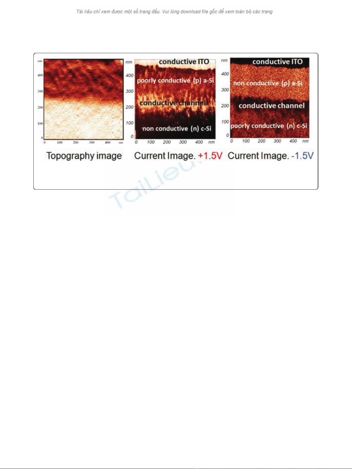
Results and discussion
In Figure 4a,b,c, an example of topography and current
images for two different biases, is presented for a (p)a-
Si:H/(n)c-Si junction. At positive bias applied to the
sample, conductive regions appear light in the current
images, while for negative bias they appear dark. The
current images clearly reveal a conductive interface layer
between the c-Si substrate and the a-Si:H film. This
layer is more conductive than both the c-Si and a-Si:H
regions. This conductive interface layer was well
observed on all samples for both (p)a-Si:H/(n)c-Si and
(n)a-Si:H/(p)c-Si heterointerfaces whatever the a-Si:H
layer thickness is. It is worth to note that the conductive
layer is not an artifact that could come from the surface
roughness. It can be clearly seen when current images
are compared with the topography one. There exists
one distinct boundary between the a-Si:H layer and c-Si
wafer, and the detected conductive channel lies within
c-Si substrate.
However, the quantitative results of the interface layer
conductivity deduced from CP-AFM measurements
Figure 2 Sketch of the CP-AFM measurements; left: setup at LGEP with the resiscope extension; right: detail of the sample
configuration and biasing.
Figure 3 Sketch of the samples prepared for (a) CP-AFM measurements and (b) planar conductance measurements.
Kleider et al.Nanoscale Research Letters 2011, 6:152
http://www.nanoscalereslett.com/content/6/1/152
Page 3 of 9
have to be considered carefully. Indeed, the reliability of
the latter is affected by the quality and nature of the
contact between the conductive tip and the sample sur-
face. The sample surface roughness, the AFM tip radius,
shape and pressure are well-known factors driving local
electrical measurements. Moreover, surface states can
induce additional band bending at the tip-surface junc-
tion modifying significantly the conductance values [5].
The CP-AFM scanning measurements can also be influ-
enced by the oxidation process after cleaving the sample
and the presence of a water meniscus between the tip
and the surface that can also lead to tip-induced oxida-
tion or trapping of carriers in localized states [6,7]. The
contact between the tip and the cleaved surface can
behave as a metal-oxide interface that then determines
the current flowing through the tip.
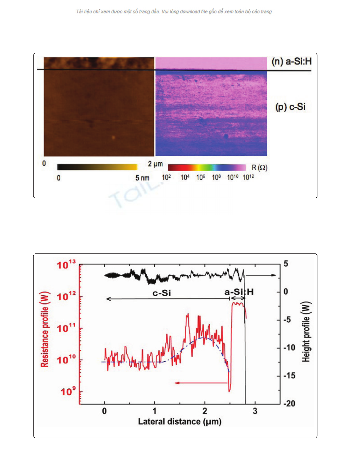
In order to minimize the effects of surface oxide and
surface states, CP-AFM measurements were performed
at LGEP under nitrogen atmosphere immediately after
having dipped the sample in an HF solution. This treat-
ment is known to passivate the silicon surface by redu-
cing the density of silicon dangling bonds, thus
minimizing the potential effect of surface states on the
surface band bending. Figure 5 illustrates an example of
topographical and electrical image of the cleaved section
obtained under these conditions with, from top to bot-
tom, the n-type a-Si:H layer (= 300 nm) and the p-type
c-Si substrate. Contrary to Figure 4, the ITO contact is
not observed since it has been partially removed after
the HF dip. Compared to results of Figure 4, with the
improved measurement procedure, a conductive channel
at the (n)a-Si:H/(p)c-Si interface is even more clearly
observed. The topographic and electrical profiles along
the heterointerface presented on Figure 6 show a flat
cleaved surface and a higher electrical contrast between
the conductive channel and both the a-Si:H layer and
the c-Si substrate. In addition, the electrical image in
the c-Si also shows a region with increasing conductivity
of about 1 μm width when sweeping away from the a-
Si:H/c-Si interface. This can be linked to the depleted
space charge region in the low-doped (p)c-Si (N
a
<10
15
cm
-3
), which has a width close to 1 μm.
The existence of an interface conductive channel has
also been evidenced by the planar conductance mea-
surements. Indeed, it was shown that the planar conduc-
tancewasordersofmagnitudelargerforthesamples
deposited on c-Si substrates (both n-andp-type) than
that measured on the a-Si:H layer deposited in the same
run on glass substrates. Activation energy of the con-
ductance for the samples deposited on glass was found
equal to about 0.35 and 0.2 eV for the (p)a-Si:H and
(n)a-Si:H layers, respectively [8,9]. These are typical
values for doped a-Si:H. The conductance for samples
deposited on c-Si had much lower activation energy, as
can be seen in Figure 7. This high planar conductance
measured on the samples deposited on c-Si is in very
good agreement with the presence of the conducting
channel revealed by our CP-AFM measurements.
We attribute this thin conductive interface channel
along with the low conductance activation energy to a
strong inversion layer at the c-Si surface that is related
to the band offset at the heterojunction.
In order to further demonstrate the existence of the
strong interface inversion layer and the related contribu-
tion to the conductance, we used the AFORS-HET soft-
ware [10] to evaluate the free carrier profiles. We
Figure 4 AFM pictures taken on a cleaved section of an ITO/(p)a-Si:H/(n)c-Si/ITO sample. Left: topography; middle: current image taken
at an applied bias of +1.5 V. Right: current image taken at an applied bias of -1.5 V. Typical roughness was less than 5 nm. On the
topographical image, the change in height from the dark top region to the light bottom region was of the order of 2 nm. In the current
images, the current values ranged from 60 pA to 17 nA.
Kleider et al.Nanoscale Research Letters 2011, 6:152
http://www.nanoscalereslett.com/content/6/1/152
Page 4 of 9
introduced the density of states (DOS) typical for n-type
a-Si:H (band gap E
g
= 1.75 eV) consisting of two expo-
nential band tails with characteristic energies k
B
T
C
and
k
B
T
V
of 0.055 and 0.12 eV for the conduction and
valence band, respectively, and with a pre-exponential
factor of 2 × 10
21
cm
-3
eV
-1
, and two Gaussian deep
defect distributions of donor and acceptor nature being
located at 0.58 and 0.78 eV above the top of the valence
band, respectively, with a maximum value of 8.7 × 10
19
cm
-3
eV
-1
and a standard deviation of 0.23 eV. A doping
Figure 5 Topography and electrical image obtained after HF dip at the cleaved section of an (n)a-Si:H/(p)c-Si heterojunction.Left:
topography; right: resistance image.
Figure 6 Profile of local resistance across the (n)a-Si:H/(p)c-Si interface corresponding to Figure 5.
Kleider et al.Nanoscale Research Letters 2011, 6:152
http://www.nanoscalereslett.com/content/6/1/152
Page 5 of 9


![Báo cáo seminar chuyên ngành Công nghệ hóa học và thực phẩm [Mới nhất]](https://cdn.tailieu.vn/images/document/thumbnail/2025/20250711/hienkelvinzoi@gmail.com/135x160/47051752458701.jpg)


%20--%3e%3cdefs%3e%3cstyle%3e%20.st0%20{%20fill:%20%23fff;%20}%20.st1%20{%20fill:%20%237800fa;%20}%20%3c/style%3e%3c/defs%3e%3cpath%20class='st1'%20d='M117.78,12.18H43.11c2.9,3.47,4.65,7.94,4.65,12.82,0,5.6-2.3,10.66-6.01,14.29h76.02l7.22-13.56-7.22-13.56Z'/%3e%3cg%3e%3cpath%20class='st0'%20d='M53.58,26.17h-.59v-1.46h.59v-4.96h2.83c1.78,0,2.67.94,2.67,2.82v5.76c0,1.87-.89,2.81-2.67,2.81h-2.83v-4.96ZM55.36,21.37v3.34h1.1v1.46h-1.1v3.34h1.01c.61,0,.91-.37.91-1.1v-5.93c0-.74-.3-1.1-.91-1.1h-1.01Z'/%3e%3cpath%20class='st0'%20d='M65.99,31.14h-1.8l-.31-2.07h-2.19l-.31,2.07h-1.64l1.82-11.39h2.62l1.82,11.39ZM65.28,18.04c-.25.46-.51.77-.75.94-.21.15-.47.22-.79.22-.26,0-.57-.07-.92-.22l-.38-.15c-.14-.05-.26-.07-.37-.07-.3,0-.53.18-.71.54l-.91-.68c.25-.46.51-.77.75-.94.21-.14.48-.21.79-.21.26,0,.57.07.92.21l.38.15c.14.05.26.07.37.07.3,0,.53-.18.71-.54l.91.68ZM61.91,27.52h1.73l-.87-5.76-.87,5.76Z'/%3e%3cpath%20class='st0'%20d='M74.53,26.89v1.52c0,1.91-.89,2.86-2.67,2.86s-2.67-.95-2.67-2.86v-5.93c0-1.91.89-2.86,2.67-2.86s2.67.95,2.67,2.86v1.11h-1.69v-1.22c0-.75-.31-1.12-.93-1.12s-.93.37-.93,1.12v6.15c0,.74.31,1.11.93,1.11s.93-.37.93-1.11v-1.63h1.69Z'/%3e%3cpath%20class='st0'%20d='M81.4,31.14h-1.8l-.31-2.07h-2.19l-.31,2.07h-1.64l1.82-11.39h2.62l1.82,11.39ZM75.9,19.2l1.52-1.91h1.71l1.51,1.91h-1.61l-.76-.95-.75.95h-1.61ZM77.32,27.52h1.73l-.87-5.76-.87,5.76ZM83.1,15.99l-1.76,1.91h-1.26l1.17-1.91h1.86Z'/%3e%3cpath%20class='st0'%20d='M84.86,19.75c1.78,0,2.67.94,2.67,2.82v1.48c0,1.87-.89,2.81-2.67,2.81h-.85v4.28h-1.79v-11.39h2.64ZM84.01,21.37v3.86h.85c.58,0,.87-.36.87-1.08v-1.71c0-.71-.29-1.07-.87-1.07h-.85Z'/%3e%3cpath%20class='st0'%20d='M93.51,19.75c1.78,0,2.67.94,2.67,2.82v1.48c0,1.87-.89,2.81-2.67,2.81h-.85v4.28h-1.79v-11.39h2.64ZM92.66,21.37v3.86h.85c.58,0,.87-.36.87-1.08v-1.71c0-.71-.29-1.07-.87-1.07h-.85Z'/%3e%3cpath%20class='st0'%20d='M98.8,31.14h-1.79v-11.39h1.79v4.88h2.03v-4.88h1.83v11.39h-1.83v-4.88h-2.03v4.88Z'/%3e%3cpath%20class='st0'%20d='M105.36,24.55h2.46v1.62h-2.46v3.34h3.09v1.63h-4.88v-11.39h4.88v1.63h-3.09v3.18ZM108.17,17.29l-1.76,1.91h-1.26l1.17-1.91h1.86Z'/%3e%3cpath%20class='st0'%20d='M112.2,19.75c1.78,0,2.67.94,2.67,2.82v1.48c0,1.87-.89,2.81-2.67,2.81h-.85v4.28h-1.79v-11.39h2.64ZM111.35,21.37v3.86h.85c.58,0,.87-.36.87-1.08v-1.71c0-.71-.29-1.07-.87-1.07h-.85Z'/%3e%3c/g%3e%3ccircle%20class='st1'%20cx='25'%20cy='25'%20r='20'/%3e%3cpath%20class='st0'%20d='M32.78,19.27c2.92,0,4.43,2.55,5.28,5.33l.71,2.17c.14.38-.33.75-.71.75h-5.61c.19-.33.24-.71.09-1.08l-.75-2.45c-.43-1.32-.99-2.64-1.79-3.77.75-.57,1.65-.94,2.78-.94h0ZM25,18.38c3.25,0,4.9,2.78,5.89,5.89l.76,2.45c.14.42-.33.8-.8.8h-11.69c-.42,0-.94-.38-.8-.8l.75-2.45c.99-3.11,2.64-5.89,5.89-5.89h0ZM25,11.35c1.74,0,3.11,1.37,3.11,3.11s-1.37,3.11-3.11,3.11-3.11-1.41-3.11-3.11,1.41-3.11,3.11-3.11h0ZM17.27,19.27c1.08,0,1.98.38,2.73.94-.8,1.13-1.37,2.45-1.74,3.77l-.8,2.45c-.14.38-.05.75.09,1.08h-5.56c-.42,0-.9-.38-.75-.75l.71-2.17c.9-2.78,2.41-5.33,5.33-5.33h0ZM17.27,12.91c1.51,0,2.78,1.27,2.78,2.83s-1.27,2.83-2.78,2.83-2.83-1.27-2.83-2.83,1.27-2.83,2.83-2.83h0ZM32.78,12.91c1.56,0,2.78,1.27,2.78,2.83s-1.23,2.83-2.78,2.83-2.83-1.27-2.83-2.83,1.27-2.83,2.83-2.83h0ZM27.07,28.56v.09c0,.57-.24,1.08-.61,1.46h0v.05c-.38.33-.9.57-1.46.57s-1.08-.24-1.46-.61h0c-.38-.38-.61-.9-.61-1.46v-.09h1.41v.09c0,.19.05.38.19.47v.05c.09.09.28.19.47.19s.38-.09.47-.19v-.05c.14-.09.24-.28.24-.47t-.05-.09h1.41ZM30.99,28.56v.09c0,1.65-.66,3.16-1.74,4.24-1.08,1.08-2.59,1.79-4.24,1.79s-3.16-.71-4.24-1.79l-.05-.05c-1.04-1.08-1.7-2.55-1.7-4.2v-.09h1.41v.09c0,1.27.47,2.4,1.27,3.25h.05c.85.85,1.98,1.37,3.25,1.37s2.4-.52,3.25-1.37c.85-.8,1.37-1.98,1.37-3.25v-.09h1.37ZM34.99,28.56v.09c0,2.78-1.13,5.28-2.92,7.07-1.79,1.79-4.29,2.92-7.07,2.92s-5.23-1.13-7.07-2.92c-1.79-1.79-2.92-4.29-2.92-7.07v-.09h1.41v.09c0,2.4.94,4.53,2.5,6.08,1.56,1.56,3.72,2.5,6.08,2.5s4.52-.94,6.08-2.5c1.56-1.56,2.5-3.68,2.5-6.08v-.09h1.41Z'/%3e%3c/svg%3e)