
NANO REVIEW Open Access
Scanning tip measurement for identification of
point defects
László Dózsa
1*
, György Molnár
1
, Vito Raineri
2
, Filippo Giannazzo
2
, János Ferencz
1
,Štefan Lányi
3
Abstract
Self-assembled iron-silicide nanostructures were prepared by reactive deposition epitaxy of Fe onto silicon.
Capacitance-voltage, current-voltage, and deep level transient spectroscopy (DLTS) were used to measure the
electrical properties of Au/silicon Schottky junctions. Spreading resistance and scanning probe capacitance
microscopy (SCM) were applied to measure local electrical properties. Using a preamplifier the sensitivity of DLTS
was increased satisfactorily to measure transients of the scanning tip semiconductor junction. In the Fe-deposited
area, Fe-related defects dominate the surface layer in about 0.5 μm depth. These defects deteriorated the Schottky
junction characteristic. Outside the Fe-deposited area, Fe-related defect concentration was identified in a thin layer
near the surface. The defect transients in this area were measured both in macroscopic Schottky junctions and by
scanning tip DLTS and were detected by bias modulation frequency dependence in SCM.
Introduction
Nanostructures require investigation of local electrical
characteristics with high spatial resolution [1]. Non-
destructive measurement of the surface and the inter-
faces is critical in SOI materials [2], such techniques are
technologically important in characterization of growth
processes [3] and in measurement of dielectric layers
[4]. Defect identification was investigated in detail using
few millimeter size electrodes [5]. Metal silicide films
have attracted attention because of their scientific curi-
osity and technical importance [6]. Fe is a critical con-
tamination in silicon and investigation of the defects
related to Fe is technologically important. In earlier stu-
dies we have investigated microscopic, structural, and
electric properties of FeSi
2
layers [7-10]. Noise and deep
level transient spectroscopy (DLTS) investigation of b-
FeSi
2
quantum dots embedded in silicon show that
Schottky junctions are not effective in evaluating defects
in the Fe-Si system since the device current is described
by space charge limited current and the depleted layer
model is not applicable [11]. Scanning probe capacitance
microscopy (SCM) was applied to measure the local
electrical characteristics; however, the isolated quantum
dots could not be resolved due to the large
concentration of Fe-related defects. The results show
that for understanding the electrical properties of nanos-
tructures the measurement of electric transport on
nanoscale is necessary. In an earlier study we have
shown that the SCM transient on the silicon surface
near the Fe-contaminated region indicates surface con-
tamination [7].
In this study we identify defects outside the Fe-deposited
region by DLTS and demonstrate the possibility of nanos-
cale defect identification by scanning tip DLTS. It is
shown that SCM modulation frequency dependence prop-
erly indicated point defects.
Sample preparation and measurements
N-type (100)-oriented Si wafers were used as substrates.
ThebacksidewasimplantedbyP
31
+ (40 keV, 480 μC),
cleaned by plasma and wet cleaning processes and
annealed at 900°C for 30 min in N
2
ambient. Before
loading the samples into the UHV evaporation chamber,
their surface was refreshed in diluted HF. The time
elapsed after cleaning to reach 1 Pa pressure in the
UHV chamber was about 30 min. After evacuation
down to 1 × 10⁻⁶ Pa and prior to evaporation, Si wafers
were annealed in situ for 5 min at 800°C. Iron has been
evaporated from ingots of 99.9% purity using an
electron gun at a pressure of 3 × 10⁻⁶ Pa by RDE pro-
cess at 0.015 nm/s rate onto the 600°C substrate, and
further annealed for 5 min at the same temperature.
* Correspondence: dozsa@mfa.kfki.hu
1
Research Institute for Technical Physics and Materials Sciences, P.O. 49, H-
1525 Budapest, Hungary
Full list of author information is available at the end of the article
Dózsa et al.Nanoscale Research Letters 2011, 6:140
http://www.nanoscalereslett.com/content/6/1/140
© 2011 Dózsa et al; licensee Springer. This is an Open Access article distributed under the terms of the Creative Commons Attribution
License (http://creativecommons.org/licenses/by/2.0), which permits unrestricted use, distribution, and reproduction in any medium,
provided the original work is properly cited.
Contamination was indicated outside the Fe deposition
by SCM [7]. To identify this contamination by DLTS
half of the Si wafer fragment was covered during Fe
deposition and 400 μm × 400 μm rectangular Au dots
Schottky junctions were prepared both in and outside
the Fe-deposited area.
SCM was measured by a DI 300 nanoscope equipped
with scanning capacitance facility. The capacitance is
measured at 1 GHz. The local dC/dV is measured using
lock-intechniquewithbiasmodulationinthe5-120
kHz range [7]. The heavily doped silicon tip covered by
a thin diamond layer, an air gap, and the conductive
substrate are evaluated as a simple MOS structure. In
this approximation the measured local dC/dV is usually
interpreted as dopant concentration under the tip. C-V,
I-V, and DLTS characteristics were measured in a
SEMILAB 83D system. A preamplifier was developed
for the capacitance input of the DLS83D equipment. A
100-nm radius tungsten tip connected directly to the
preamplifier input was positioned above the silicon sur-
face. The apparent capacitance was amplified 200 times
as it was calibrated by measuring 1 and 5 pF standard
capacitances with and without the preamplifier. The
amplification of capacitance without increased noise is
possible since the low noise preamplifier decouples the
load of the measuring cables from the measuring tip.
This method will be referred to as scanning tip DLTS.
The spreading resistance (SR) was measured in an
SSM130 system using two measuring tips at 100 μm dis-
tance. A series of clean silicon with doping in the 0.08-
180 Ωcm range were used to calibrate the SR
measurement.
Results
Electrical characteristics of Schottky junctions
The I-Vcharacteristics of Schottky junctions in the Fe-
deposited area at room temperature were dominated by
the series resistance and leakage. The series resistance
on the Fe-deposited area has a high scatter. The
Schottky junction prepared on silicon outside the Fe-
deposited area has 0.73 V built-in voltage and is appro-
priate for identification of defects by DLTS. SR measure-
ments were carried out on beveled samples of the
Fe-deposited area. It shows that the resistivity in the
Fe-deposited region is an order of magnitude higher in
about 0.3-0.4 μm depth. The resistivity in the Fe-depos-
ited region has shown large scatter. The silicon in about
1μm depth below the Fe deposition exhibits resistivity
appropriate for the silicon starting wafer.
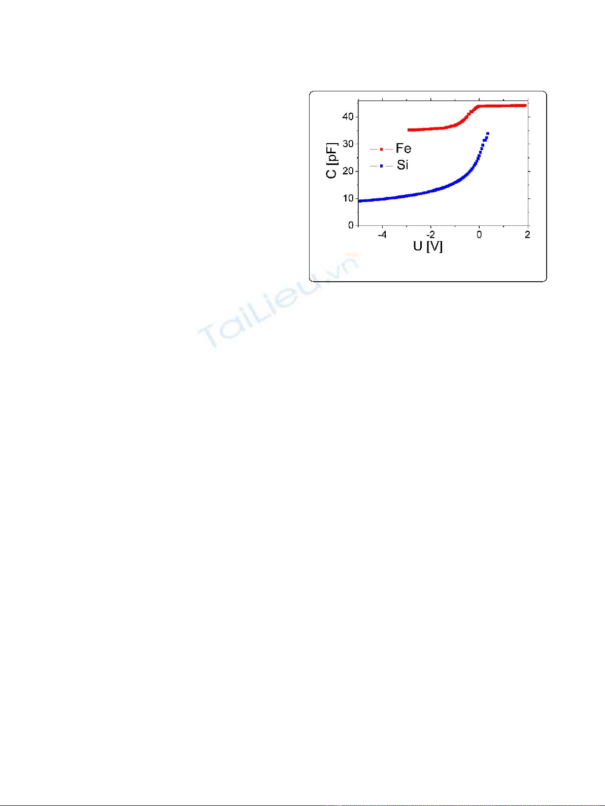
The C-Vcharacteristics of a Schottky junction pre-
pared on the Fe-deposited area and on the free silicon
are shown in Figure 1. The capacitance of the Schottky
junction on the Fe-deposited area is larger, indicating
that the Fe-generated defect concentration in this area
in about 0.5 μm depth is few time 10
16
/cm
3
. This defect
concentration is an order of magnitude larger than the
2×10
15
/cm
3
doping determined from the 1/C
2
-Vplot
measured in junctions prepared on the silicon surface.
These defects are donor type deep level defects, situated
about 250-300 meV below the conduction band edge.
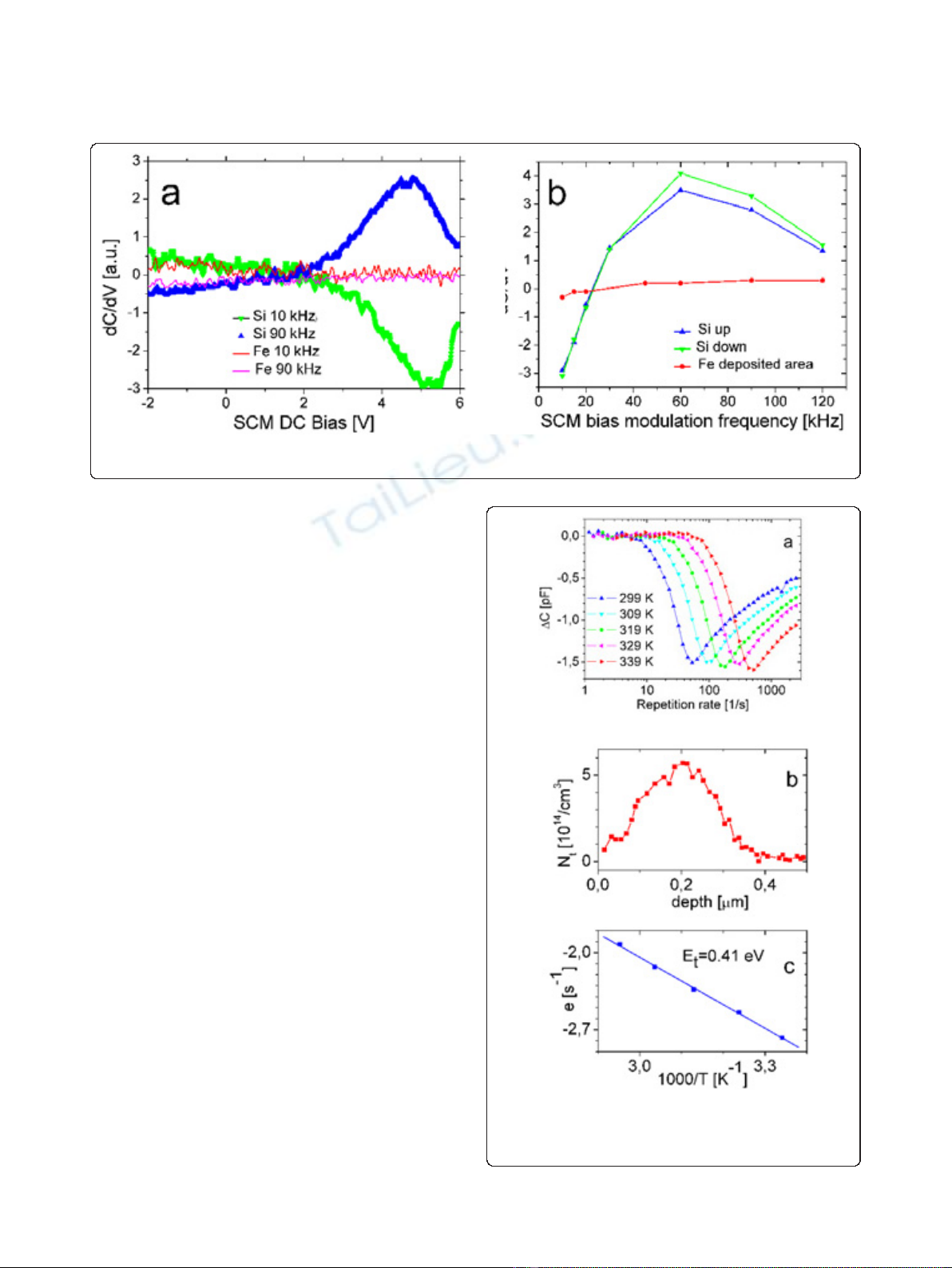
Scanning capacitance measurements
In the Fe-deposited area SCM has shown a patterned
surface on the 1 μm scale. The SCM contrast was clear;
however, comparison of SCM images with secondary
electron microscopy and AFM images shows that the
quantum dots cannot be resolved by SCM [7]. A sum-
mary of the SCM measurements is shown in Figure 2.
dC/dV-bias characteristics at 10 and 90 kHz modulation
frequencies are shown in Figure 2a. The bias depen-
dence of dC/dV in the Fe-deposited area is weak as is
shown in Figure 2a. Outside the Fe-deposited area the
sign of the peak in dC/dV has changed by varying the
bias modulation frequency from 10 to 90 kHz as it is
shown in Figure 2a. The position of the peak at about 5
V bias was independent of the modulation frequency,
however, its amplitude varied with bias modulation fre-
quency as it is shown in Figure 2b. The scans repeated
with increasing and decreasing bias modulation frequen-
cies exhibited some hysteresis indicated by Si up and Si
down in Figure 2b. The change in the sign of dC/dV
can be explained by defects on the surface.
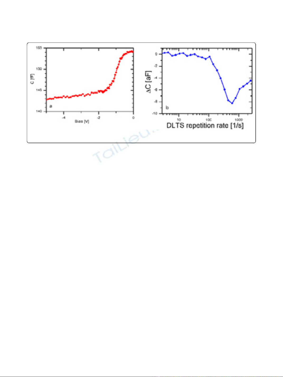
DLTS measurements
DLTS identified the Fe-related defects in the Fe-depos-
ited area; however, weak junction characteristics prevent
proper evaluation of the defects by DLTS. C-Vprofile
has shown that in the Fe-deposited area the deep defect
concentration is few times 10
16
/cm
3
, order of magnitude
larger than the doping of the starting silicon wafer in
Figure 1 C-Vcharacteristics of Schottky junction prepared in
the Fe-deposited area (Fe) and on the silicon surface (Si).
Dózsa et al.Nanoscale Research Letters 2011, 6:140
http://www.nanoscalereslett.com/content/6/1/140
Page 2 of 5
about 0.5 μmdepth,whichdoesnotsuitforDLTS
measurements.
DLTS spectra measured in a Schottky junction outside
the Fe deposition area are shown in Figure 3a. The
spectra were recorded at -5 V reverse bias and 0 V bias,
5μs filling pulses. The spectra are broad, indicating that
the defect activation energy is distributed. The depth
profile measured by DLTS is shown in Figure 3b. The
defects are localized at about 200 nm from the silicon
surface. The activation energy of the defect determined
by Arrhenius plot shown in Figure 3c agrees with a
defect attributed to Fe in silicon [12]. We remark that
the depth profile of the defect may be also interpreted
as a distributed energy surface state in 5 × 10
10
/cm
2
density, since the depth resolution of the capacitance
DLTS technique is not satisfactory to distinguish these
details.
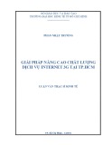
Scanning tip DLTS measurements
A measuring tip was shaped from an 80-μmdiameter
tungsten wire to an approximately 100 nm radius. It
was placed in a shield extending to about 0.5 mm from
the surface, to reduce the stray capacitance. The tip was
positioned as near as possible without measurable
current (few pA) through the tip-wafer junction. It
represents an MIS structure. In the Fe-deposited area
the tip-wafer capacitance did not depend on the applied
bias and no DLTS signal was detected. It is explained by
the high defect concentration surface layer.
The measured scanning tip C-Vcharacteristic outside
the Fe deposition is shown in Figure 4a. The scanning
tip DLTS frequency scan spectrum measured in the
same position is shown in Figure 4b. The spectra were
measured at room temperature. The spectra measured
in different position on the surface show a scatter in
Figure 2 SCM signal measured on the Fe-deposited area and on the silicon surface.a. dC/dV-voltage plots at 10 and 90 kHz bias. b.
Dependence of the amplitude of the dC/dV peak at about +5 V on the bias modulation frequencies.
Figure 3 DLTS results in macroscopic Schottky junctions.a.
DLTS frequency scan spectra measured by DLS-83D system. b.
Depth profile of the defect. c. Arrhenius plot for determination of
the activation energy of the defect.
Dózsa et al.Nanoscale Research Letters 2011, 6:140
http://www.nanoscalereslett.com/content/6/1/140
Page 3 of 5
amplitude and peak position. This property is analogous
to the large scatter observed by SCM outside the Fe
deposition area, and the scatter of the DLTS spectra
measured in different position Schottky junctions.
Discussion
The above results were measured in a wide frequency
range from DC to 1 GHz range, and with contact size
from few tens of nanometers to 400 μm. SCM capacitance
measured at 1 GHz is limited by the relaxation time of
defects. Only the free carriers in the bulk silicon can follow
this excitation. For this reason the deep-level defects can
be detected only on the free silicon surface, since defects
in the Fe-deposited region have much larger time constant
than 1 ns. The Fe-related defects may influence the space
charge in the 5-120 kHz modulation frequency range at
room temperature. SCM detects an electrically overlap-
ping network of conductive quantum dots on the Fe-
deposited area. The capacitance measurements at 1 MHz
indicate an about 0.5 μm wide defective layer on the Fe-
deposited area. The defective layer is due to large concen-
tration of Fe-related defects which can follow only the low
frequency excitation. In the capacitance transient mea-
surements(1MHzinDLTSand1GHzinSCM)these
defects do not follow the bias modulation, but these
defects dominate the steady state I-V,C-V,andSR
measurements.
On the free silicon surface at low bias modulation fre-
quency (below 20-30 kHz) in SCM dC/dV the Fe-
related defect can follow the modulation but at higher
frequency only the free carriers follow the excitation,
and dC/dV gives n-type silicon doping. It is analogous
to the admittance spectroscopy in macroscopic junc-
tions [13,14]. The scanning tip DLTS spectra are similar
tolargeareaSchottkyjunctions.Theresultsdemon-
strate that SCM and scanning tip DLTS are able to
identify defects in semiconductors with high spatial
resolution.
Conclusion
FeSi
2
quantum dots were grown by in situ self-organized
growth process on silicon. In the Fe-deposited layer a
resistive layer with high concentration of defects domi-
nates the characteristics; charge captured on these
defects can follow only the low frequency modulation.
The concentration of the Fe-related deep-level defects
generated outside the Fe-deposited region was found in
about 5 × 10
14
/cm
3
concentration near the surface.
These Fe-related defects are localized at about 200 nm
depth from the surface and may be interpreted also as
distributed energy surface state defects in about 2 ×
10
10
/cm
2
concentration. Scanning tip capacitance DLTS
spectra on the free silicon surface are analogous to
those measured in Schottky junctions. The defects are
indicated by the modulation frequency dependence of
the SCM dC/dV signal, showing a tool to detect point
defects on microscopic scale by SCM.
Abbreviations
DLTS: deep level transient spectroscopy; SCM: scanning probe capacitance
microscopy; SR: spreading resistance.
Acknowledgements
This study was performed with financial support by OTKA grant (Hungary)
No. K81998, by the SK-HU-0024-08 project of Slovakian-Hungarian, and SK-IT-
0020-08 project of Slovakian-Italian scientific cooperation agreements.
Author details
1
Research Institute for Technical Physics and Materials Sciences, P.O. 49, H-
1525 Budapest, Hungary
2
CNR-IMM, Strada VIII 5, 95121 Catania, Italy
Figure 4 Electrical characteristics measured by the capacitance preamplifier with a 100 nm radius tip positioned near the silicon
surface.a. C-Vcharacteristics. b. DLTS frequency scan.
Dózsa et al.Nanoscale Research Letters 2011, 6:140
http://www.nanoscalereslett.com/content/6/1/140
Page 4 of 5

3
Institue of Physics, Slovakian Academy of Sciences, Dúbravská cesta 9, SK-
845 11 Bratislava, Slovakia
Authors’contributions
FG and VR carried our the SCM experiment, GM prepared the investigated
structures and participated in the plan of the study, SL participated in the
design and has built the preamplifier and piezo positioner, JF measured the
spreading resistance, LD measured DLTS and participated in the design of
the preamplifier and plan of study
Competing interests
The authors declare that they have no competing interests.
Received: 30 September 2010 Accepted: 14 February 2011
Published: 14 February 2011
References
1. Hasegawa H, Sato T, Kasai S, Adamowicz B, Hashizume T: Dynamics and
control of recombination process at semiconductor surfaces, interfaces
and nano-structures. Solar Energy 2006, 80:629.
2. Okumura T, En A, Eguchi K, Suhara M: Contactless characterization of
surface and interface band-bending in Silicon-On-Insulator (SOI)
structures. Mater Sci Eng B 2002, 91:182.
3. Takahashi H, Yoshida T, Mutoh M, Sakai T, Hasegawa H: In-situ
characterization technique of compound semiconductor heterostructure
growth and device processing steps based on UHV contactless
capacitance-voltage measurement. Solid State Electron 1999, 43:1561.
4. Fumagalli L, Ferrari G, Sampietro M, Gomila G: Dielectric-constant
measurement of thin insulating films at low frequency by nanoscale
capacitance microscopy. Appl Phys Lett 2007, 91:243110.
5. Yoshida G, Nakashishi R, Kishino S: Sensitivity of contactless transient
spectroscopy and actual measurement of localized states in oxidized Si
wafer. J Cryst Growth 2000, 210:379.
6. Reader AH, van Ommen AH, Weijs PJW, Wolters RAM, Oostra DJ: Transition
metal silicides in silicon technology. Rep Prog Phys 1992, 56:1397.
7. Dózsa L, Molnár G, Horváth ZJ, Tóth AL, Gyulai J, Raineri V, Giannazzo F:
Investigation of the morphology and electrical characteristics of FeSi2
quantum dots on silicon. Appl Surf Sci 2004, 234:60.
8. Dózsa L, Horváth E, Molnár G, Tóth AL, Vértesy Z, Vázsonyi E, PetőG:
Characteristics of FeSi2 quantum dots on silicon. Eur Phys J Appl Phys
2004, 27:85.
9. Vouroutzis N, Zorba TT, Dimitriadis CA, Paraskevopoulos KM, Dózsa L,
Molnár G: Thickness dependent structure of β-FeSi2 grown on silicon by
solid phase epitaxy. J Alloys Compd 2005, 393:167.
10. Vouroutzis N, Zorba T, Dimitriadis CA, Paraskevopoulos KM, Dózsa L,
Molnár G: Growth of β-FeSi2 particles on silicon by reactive deposition
epitaxy. J Alloys Compd 2008, 448:202.
11. Tsormpatzoglou A, Thassis DH, Dimitriadis CA, Dózsa L, Galkin NG,
Goroshko DL, Polyarnyi VO, Chusovitin EA: Deep levels in silicon Schottky
junctions with embedded arrays of β-FeSi2 nanocrystallites. J Appl Phys
2006, 100:0733139.
12. Wünstel K, Wagner P: Iron-related deep levels in silicon. Solid State
Commun 1961, 40:797.
13. Schmidt C: Photoconductivity and Hall-effect of iron-diffused silicon. Appl
Phys 1978, 17:137.
14. Losee L: Admittance spectroscopy of impurity levels in Schottky barriers.
J Appl Phys 1975, 46:2204.
doi:10.1186/1556-276X-6-140
Cite this article as: Dózsa et al.: Scanning tip measurement for
identification of point defects. Nanoscale Research Letters 2011 6:140.
Submit your manuscript to a
journal and benefi t from:
7 Convenient online submission
7 Rigorous peer review
7 Immediate publication on acceptance
7 Open access: articles freely available online
7 High visibility within the fi eld
7 Retaining the copyright to your article
Submit your next manuscript at 7 springeropen.com
Dózsa et al.Nanoscale Research Letters 2011, 6:140
http://www.nanoscalereslett.com/content/6/1/140
Page 5 of 5


%20--%3e%3cdefs%3e%3cstyle%3e%20.st0%20{%20fill:%20%23fff;%20}%20.st1%20{%20fill:%20%237800fa;%20}%20%3c/style%3e%3c/defs%3e%3cpath%20class='st1'%20d='M117.78,12.18H43.11c2.9,3.47,4.65,7.94,4.65,12.82,0,5.6-2.3,10.66-6.01,14.29h76.02l7.22-13.56-7.22-13.56Z'/%3e%3cg%3e%3cpath%20class='st0'%20d='M53.58,26.17h-.59v-1.46h.59v-4.96h2.83c1.78,0,2.67.94,2.67,2.82v5.76c0,1.87-.89,2.81-2.67,2.81h-2.83v-4.96ZM55.36,21.37v3.34h1.1v1.46h-1.1v3.34h1.01c.61,0,.91-.37.91-1.1v-5.93c0-.74-.3-1.1-.91-1.1h-1.01Z'/%3e%3cpath%20class='st0'%20d='M65.99,31.14h-1.8l-.31-2.07h-2.19l-.31,2.07h-1.64l1.82-11.39h2.62l1.82,11.39ZM65.28,18.04c-.25.46-.51.77-.75.94-.21.15-.47.22-.79.22-.26,0-.57-.07-.92-.22l-.38-.15c-.14-.05-.26-.07-.37-.07-.3,0-.53.18-.71.54l-.91-.68c.25-.46.51-.77.75-.94.21-.14.48-.21.79-.21.26,0,.57.07.92.21l.38.15c.14.05.26.07.37.07.3,0,.53-.18.71-.54l.91.68ZM61.91,27.52h1.73l-.87-5.76-.87,5.76Z'/%3e%3cpath%20class='st0'%20d='M74.53,26.89v1.52c0,1.91-.89,2.86-2.67,2.86s-2.67-.95-2.67-2.86v-5.93c0-1.91.89-2.86,2.67-2.86s2.67.95,2.67,2.86v1.11h-1.69v-1.22c0-.75-.31-1.12-.93-1.12s-.93.37-.93,1.12v6.15c0,.74.31,1.11.93,1.11s.93-.37.93-1.11v-1.63h1.69Z'/%3e%3cpath%20class='st0'%20d='M81.4,31.14h-1.8l-.31-2.07h-2.19l-.31,2.07h-1.64l1.82-11.39h2.62l1.82,11.39ZM75.9,19.2l1.52-1.91h1.71l1.51,1.91h-1.61l-.76-.95-.75.95h-1.61ZM77.32,27.52h1.73l-.87-5.76-.87,5.76ZM83.1,15.99l-1.76,1.91h-1.26l1.17-1.91h1.86Z'/%3e%3cpath%20class='st0'%20d='M84.86,19.75c1.78,0,2.67.94,2.67,2.82v1.48c0,1.87-.89,2.81-2.67,2.81h-.85v4.28h-1.79v-11.39h2.64ZM84.01,21.37v3.86h.85c.58,0,.87-.36.87-1.08v-1.71c0-.71-.29-1.07-.87-1.07h-.85Z'/%3e%3cpath%20class='st0'%20d='M93.51,19.75c1.78,0,2.67.94,2.67,2.82v1.48c0,1.87-.89,2.81-2.67,2.81h-.85v4.28h-1.79v-11.39h2.64ZM92.66,21.37v3.86h.85c.58,0,.87-.36.87-1.08v-1.71c0-.71-.29-1.07-.87-1.07h-.85Z'/%3e%3cpath%20class='st0'%20d='M98.8,31.14h-1.79v-11.39h1.79v4.88h2.03v-4.88h1.83v11.39h-1.83v-4.88h-2.03v4.88Z'/%3e%3cpath%20class='st0'%20d='M105.36,24.55h2.46v1.62h-2.46v3.34h3.09v1.63h-4.88v-11.39h4.88v1.63h-3.09v3.18ZM108.17,17.29l-1.76,1.91h-1.26l1.17-1.91h1.86Z'/%3e%3cpath%20class='st0'%20d='M112.2,19.75c1.78,0,2.67.94,2.67,2.82v1.48c0,1.87-.89,2.81-2.67,2.81h-.85v4.28h-1.79v-11.39h2.64ZM111.35,21.37v3.86h.85c.58,0,.87-.36.87-1.08v-1.71c0-.71-.29-1.07-.87-1.07h-.85Z'/%3e%3c/g%3e%3ccircle%20class='st1'%20cx='25'%20cy='25'%20r='20'/%3e%3cpath%20class='st0'%20d='M32.78,19.27c2.92,0,4.43,2.55,5.28,5.33l.71,2.17c.14.38-.33.75-.71.75h-5.61c.19-.33.24-.71.09-1.08l-.75-2.45c-.43-1.32-.99-2.64-1.79-3.77.75-.57,1.65-.94,2.78-.94h0ZM25,18.38c3.25,0,4.9,2.78,5.89,5.89l.76,2.45c.14.42-.33.8-.8.8h-11.69c-.42,0-.94-.38-.8-.8l.75-2.45c.99-3.11,2.64-5.89,5.89-5.89h0ZM25,11.35c1.74,0,3.11,1.37,3.11,3.11s-1.37,3.11-3.11,3.11-3.11-1.41-3.11-3.11,1.41-3.11,3.11-3.11h0ZM17.27,19.27c1.08,0,1.98.38,2.73.94-.8,1.13-1.37,2.45-1.74,3.77l-.8,2.45c-.14.38-.05.75.09,1.08h-5.56c-.42,0-.9-.38-.75-.75l.71-2.17c.9-2.78,2.41-5.33,5.33-5.33h0ZM17.27,12.91c1.51,0,2.78,1.27,2.78,2.83s-1.27,2.83-2.78,2.83-2.83-1.27-2.83-2.83,1.27-2.83,2.83-2.83h0ZM32.78,12.91c1.56,0,2.78,1.27,2.78,2.83s-1.23,2.83-2.78,2.83-2.83-1.27-2.83-2.83,1.27-2.83,2.83-2.83h0ZM27.07,28.56v.09c0,.57-.24,1.08-.61,1.46h0v.05c-.38.33-.9.57-1.46.57s-1.08-.24-1.46-.61h0c-.38-.38-.61-.9-.61-1.46v-.09h1.41v.09c0,.19.05.38.19.47v.05c.09.09.28.19.47.19s.38-.09.47-.19v-.05c.14-.09.24-.28.24-.47t-.05-.09h1.41ZM30.99,28.56v.09c0,1.65-.66,3.16-1.74,4.24-1.08,1.08-2.59,1.79-4.24,1.79s-3.16-.71-4.24-1.79l-.05-.05c-1.04-1.08-1.7-2.55-1.7-4.2v-.09h1.41v.09c0,1.27.47,2.4,1.27,3.25h.05c.85.85,1.98,1.37,3.25,1.37s2.4-.52,3.25-1.37c.85-.8,1.37-1.98,1.37-3.25v-.09h1.37ZM34.99,28.56v.09c0,2.78-1.13,5.28-2.92,7.07-1.79,1.79-4.29,2.92-7.07,2.92s-5.23-1.13-7.07-2.92c-1.79-1.79-2.92-4.29-2.92-7.07v-.09h1.41v.09c0,2.4.94,4.53,2.5,6.08,1.56,1.56,3.72,2.5,6.08,2.5s4.52-.94,6.08-2.5c1.56-1.56,2.5-3.68,2.5-6.08v-.09h1.41Z'/%3e%3c/svg%3e)