
NANO EXPRESS Open Access
The role of the surfaces in the photon absorption
in Ge nanoclusters embedded in silica
Salvatore Cosentino
1
, Salvatore Mirabella
1*
, Maria Miritello
1
, Giuseppe Nicotra
2
, Roberto Lo Savio
1
,
Francesca Simone
1
, Corrado Spinella
2
, Antonio Terrasi
1
Abstract
The usage of semiconductor nanostructures is highly promising for boosting the energy conversion efficiency in
photovoltaics technology, but still some of the underlying mechanisms are not well understood at the nanoscale
length. Ge quantum dots (QDs) should have a larger absorption and a more efficient quantum confinement effect
than Si ones, thus they are good candidate for third-generation solar cells. In this work, Ge QDs embedded in silica
matrix have been synthesized through magnetron sputtering deposition and annealing up to 800°C. The thermal
evolution of the QD size (2 to 10 nm) has been followed by transmission electron microscopy and X-ray diffraction
techniques, evidencing an Ostwald ripening mechanism with a concomitant amorphous-crystalline transition. The
optical absorption of Ge nanoclusters has been measured by spectrophotometry analyses, evidencing an optical
bandgap of 1.6 eV, unexpectedly independent of the QDs size or of the solid phase (amorphous or crystalline). A
simple modeling, based on the Tauc law, shows that the photon absorption has a much larger extent in smaller
Ge QDs, being related to the surface extent rather than to the volume. These data are presented and discussed
also considering the outcomes for application of Ge nanostructures in photovoltaics.
PACS: 81.07.Ta; 78.67.Hc; 68.65.-k
Introduction
Nanostructured materials represent a promising route of
development for photovoltaics (PV) because of the
unique optical and electronic properties caused by the
quantum confinement of electrons and holes, allowing
to increase the efficiency of the sunlight-electricity con-
version [1-8]. It has been argued that quantum dots
(QDs) permit to gather a great part of solar energy in a
variety of modes, among which multiple exciton genera-
tion [1,6], intermediate band formation [7], or modula-
tion of the solar absorption based on the size tuning
due to the quantum confinement effect (QCE) [8]. Actu-
ally, confined Si (2- to 5-nm QDs) shows a threshold for
light absorption (optical bandgap, E
gopt
spanning over
2.0 to 2.8 eV [9,10], well larger than that of bulk Si (1.1
eV) [11]. Since the actual PV module production is lar-
gely dominated by Si (mono, poly-crystalline, or amor-
phous), the enhancement of energy conversion efficiency
through Si-based or Si-compatible nanostructures could
lead to a breakthrough in the PV market.
Recently, the variation of the Si QD optical bandgap
was experimentally shown to rely not only on the size
tuning but also on the deposition technique (comparing
sputtering and chemical vapor deposition methods) and
on the amorphous-crystalline (a-c)phaseofthe
nanoclusters [10]. Moreover, theoretical calculations
confirmed that the amorphization of Si nanoclusters
reduces the fundamental gap and increases the absorp-
tion strength [12,13]. Some trial PV devices have been
fabricated with Si QDs (size of 3 to 8 nm) embedded in
SiO
2
, exhibiting a conversion efficiency up to 10% [14].
In similar devices, a poor carrier transport has been evi-
denced as a limiting factor for cell performance and a
maximum open circuit voltage of 410 mV was mea-
sured, well below that of single-junction mono-crystal-
line Si solar cell [15]. Thus, at present, PV cells based
on Si QDs do not show encouraging characteristics. On
the other hand, passing from bulk to confined Si, E
gopt
hops from 1.1 to about 2.0 eV, opening a not-negligible
break in the solar energy harvesting by Si. Thus, new
* Correspondence: mirabella@ct.infn.it
1
MATIS-IMM-CNR and Dipartimento di Fisica e Astronomia, Università di
Catania, Via Santa Sofia 64, 95123 Catania, Italy
Full list of author information is available at the end of the article
Cosentino et al.Nanoscale Research Letters 2011, 6:135
http://www.nanoscalereslett.com/content/6/1/135
© 2011 Salvatore et al; licensee Springer. This is an Open Access article distributed under the terms of the Creative Commons
Attribution License (http://creativecommons.org/licenses/by/2.0), which permits unrestricted use, distribution, and reproduction in
any medium, provided the original work is properly cited.

nanostructured materials, Si compatible, are required to
fill this gap.
Recently, Ge QDs are attracting a larger attention for
their potential applications in PV because of the lower
fabrication temperature and of the larger excitonic Bohr
radius (approximately 20 nm) with respect to Si
(approximately 5 nm) [11,16], this allowing in principle
an easier modulation of the electronic properties by the
QCE. Moreover, since the electronic bandgap of bulk
Ge (0.66 eV) is well lower than that of bulk Si (1.1 eV)
[11], the QCE in Ge QDs could allow the modulation of
E
gopt
within the energy range (1.1 to 2.0 eV) where bulk
or confined Si fails. Up to now, Ge QDs embedded in
SiO
2
have been widely studied for optoelectronic appli-
cations [16-20], with a nearly size-independent photolu-
minescence which was not attributed to simple
confinement effect but probably to the QD/matrix inter-
face [16,19]. Only a few studies have been performed on
nanoscaled Ge clusters for PV application, mainly
focused on their fabrication within SiO
2
matrix [21,22],
or on the combination with titania nanoparticles [23]. In
addition, the sunlight absorption in these nanostructures
has been poorly characterized, and a univocal consensus
on the underlying mechanism has not been reached.
The absorption spectrum (a)ofGeQDshasbeen
experimentally measured, and it was shown that the two
main peaks visible in aof bulk Ge (i.e., the E
1
and E
2
direct transitions at 2.1 and 4.3 eV, related to the band
structure of bulk Ge [24]) disappear by shrinking the
QD size below 3 nm, suggesting that the band structure
of bulk can be altered by the confinement [25]. Later
on, Tognini and co-workers evidenced a relevant blue-
shift of E
2
(due to the QCE) and a weakening of E
1
with
size reduction of Ge QDs embedded in Al
2
O
3
[26],
while Heath et al. concluded that E
1
and E
2
transitions
areapparentlyunaffectedbyconfinementinGeQDs
produced with ultrasonic methods [27]. For PV applica-
tion, the E
gopt
of embedded Ge QDs is a crucial para-
meter, but experimental measurements are still lacking.
Several theoretical studies predict that it increases up to
5 eV by reducing the QD size below 1 nm, while it is
fairly constant at a value of 1.5 eV for size larger than 6
nm [28,29].
In order to verify these calculation results and to test
the application of Ge QDs for PV, some open questions
are whether the size of such nanostructures is the only
parameter determining the sunlight absorption and to
which extent, and whether there is some effect related
to the structural phase (aor c) of Ge QD or to the QD-
matrix interfaces. In this paper, we report an experimen-
tal investigation on the photon absorption in Ge QDs (2
to 10 nm in size) embedded in silica, providing the ther-
mal evolution of the absorption spectra in connection
with the a-ctransition and the QD ripening. An optical
bandgap of 1.6 eV has been found with clear evidence
that light absorption is mediated by electronic states
localized at the interface between Ge QDs and the host-
ing matrix.
Experimental
Ge QDs embedded in silica have been obtained by mag-
netronco-sputtering of SiO
2
and Ge targets (Ar atmo-
sphere,nominal deposition temperature 400°C), upon
fused silicasubstrates. Thermal annealing in the 600°C to
800°C range(1 h, N
2
ambient) promoted the phase
separation of SiGeOfilm into SiO
2
,GeO
2
,andGeclus-
ters (due toprecipitation of the exceding Ge). The thick-
ness of the SiGeO film (approximately 280 nm) was
measured by transmission electron microscopy (TEM),
and the elemental composition was determined by
Rutherford backscattering spectrometry (RBS, 2.0 MeV
He
+
beam). The spectra, simulated with SIMNRA soft-
ware [30], revealed that in the as-deposited sample, the
Si, Ge, and O contents are 24, 16, and 60 at.%, respec-
tively, homogeneous in depth. Because of the annealing,
the overall Ge amount contained in the SiGeO film
slightly decreases from 3.0 × 10
17
cm
-2
(in the as-depos-
ited sample) to 2.6 × 10
17
cm
-2
(800°C-annealed sample)
due to the Ge out-diffusion through the surface, as
already evidenced in the literature [20]. Normal trans-
mittance (T) and the 20° reflectance (R) spectra in the
200- to 2000-nm wavelength range were measured, by
using a Varian Cary 500 double beam scanning UV/
Visible/NIR spectrophotometer (Agilent Technologies,
Inc., Santa Clara, CA, USA) for extracting the absorp-
tion coefficient of the films, as described in Ref. [10].
Cross-section transmission electron microscopy in high
resolution (HR-TEM) or scanning mode (STEM) was
used to verify the formation of Ge clusters, to measure
their size distribution, and to evidence the crystalline
phase. The observations were carried out using a JEOL
2010F microscope (JEOL Ltd., Tokyo,Japan) operating at
200 kV equipped with a Schottky field-emission gun, a
Gatan imaging filter (GIF) for compositional mappings,
and a JEOL STEM unit, with an annular dark-field
detector operated in high angle (HAADF) mode for Z
contrast imaging. In addition, c-Ge clusters have been
characterized also with glancing-incidence X-ray diffrac-
tion (GI-XRD) analysis, using the K
a
radiation of Cu
(l= 0.154 nm), fixing the incidence angle at 0.5° and
performing the 2θscan. Basing on the (111), (110), and
(220) Bragg diffraction peaks of the GI-XRD spectra
(not shown), the average QD size was estimated by
applying the Scherrer formula [31].
Results and discussion
A high density of Ge precipitates within the SiO
2
matrix is
revealed by the STEM images (at the same magnification)
Cosentino et al.Nanoscale Research Letters 2011, 6:135
http://www.nanoscalereslett.com/content/6/1/135
Page 2 of 7
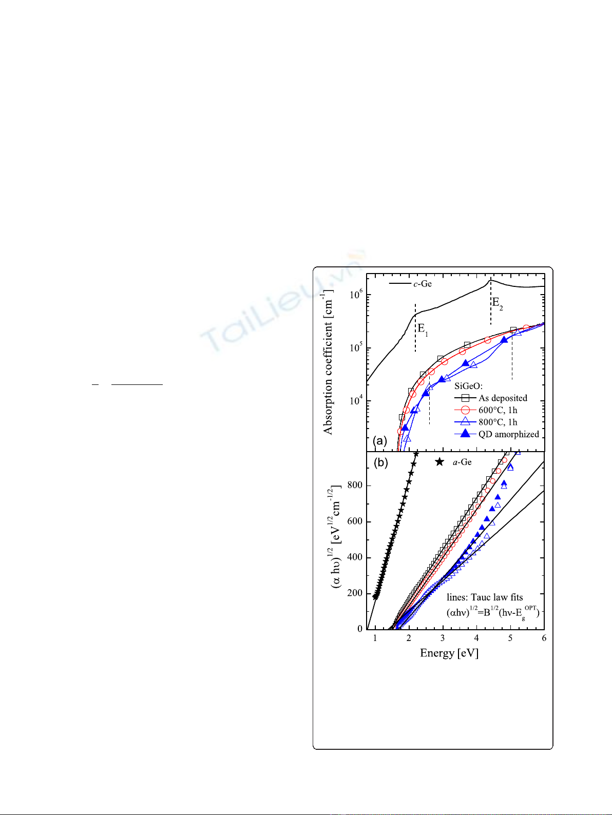
in Figure 1, just after the deposition (a) and after thermal
annealing at 750°C (b). The bright patches represent Ge
nanoclusters whose density and mean size noticeably
change after annealing (the mean diameter increasing
from 2.5 to 7.5 nm). Although Ge QDs are already present
in the as-deposited films, as recently found also by Zhang
et al. [22], the deposition temperature was not high
enough to induce the formation of crystalline QDs in our
case. SiGeO film deposited by sputtering can be described
as a mixture of Ge, GeO
2
, and SiO
2
units, according to a
random matrix model, similarly to what occurs for silicon-
rich oxide [32]. During annealing, Ge QDs undergo an
Ostwald ripening mechanism, similar to the Si QD case
[33], leading to a size increasing of precipitates with a con-
comitant a-ctransition occurring in the 600°C to 800°C
range [20]. The inset in Figure 1b reports an HR-TEM
image of the annealed sample, evidencing a clear crystal-
line phase for Ge QD with the fringes due to crystalline
planes (indicated by red lines and separated by 0.33 nm, as
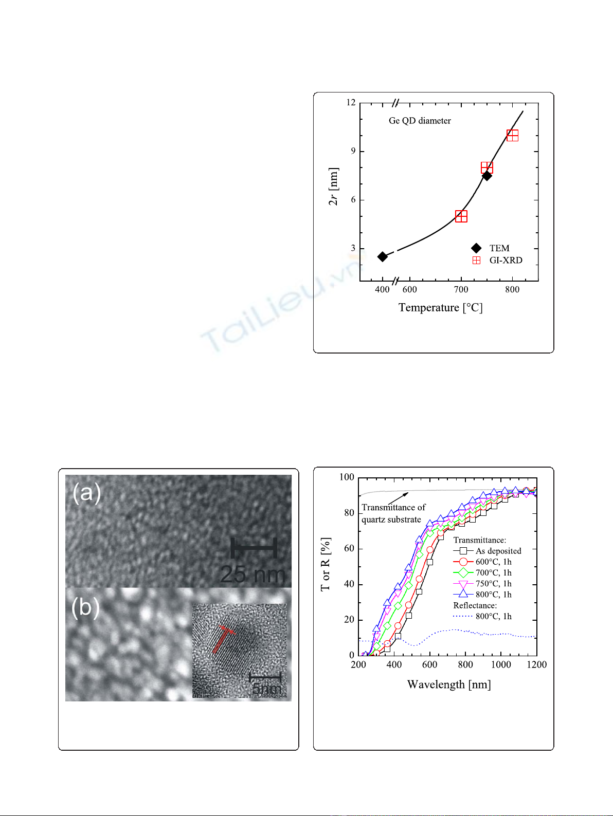
the (111) planes of c-Ge bulk). In Figure 2, the mean QD
diameter (2r) measured by TEM (diamond) and by GI-
XRD (crossed squares, line is a guide for eyes) is reported
as a function of the annealing temperature. Even if GI-
XRD gives information only on c-QDs, the reasonable
agreement between the two techniques observed at 750°C
is supporting the idea that the size distribution of c-QDs
does not significantly deviate from that of a-QDs. The
overall variation of rcan be extracted by joining the two
techniques, showing a clear QD enlargement in the 400°C
to 800°C range compatible with an Ostwald ripening
mechanism.
In Figure 3, the transmittance (T) spectra of some
SiGeO samples are plotted (symbols) together with that
of the quartz substrate (T~ 90%, the missing 10% being
due to reflection by the quartz surface, not reported
here).ThepresenceofGeQDsinduces,inthe200to
Figure 1 Cross sectional dark-field STEM images (same
magnification) of the sample. As deposited (a) or after annealing
at 750°C (b). The inset reports a HR-TEM of the annealed sample,
showing the presence of a clear crystalline structure.
Figure 2 Thermal evolution of the mean diameter (2r)ofGe
nanostructures. Measured by TEM (diamond) or GI-XRD (squares).
Line is a guide for eyes (color online).
Figure 3 Transmittance and reflectance spectra. Transmittance
spectra for the bare substrate (quartz, continuous line) and for the
as-deposited and annealed SiGeO samples (symbols). The
reflectance spectrum (R) for the SiGeO sample after annealing at
800°C is also reported (dotted line) (color online).
Cosentino et al.Nanoscale Research Letters 2011, 6:135
http://www.nanoscalereslett.com/content/6/1/135
Page 3 of 7
1000 nm range, a strong decrease of Twhich is modu-
lated with the annealing temperature. On the other
hand, the reflectance (R) spectrum does not depend on
the temperature (thus, only the 800°C-annealed sample
was reported) and Ris quite low (approximately 10%)
and constant, except for the typical oscillations caused
by the beam interference at the air-SiGeO and SiGeO-
quartz interfaces. The decrease of Tfor wavelengths
smaller than approximately 1000 nm shows the absorp-
tion of light related to thepresenceofGeQDs
embedded in the film. On the other hand, the blueshift
of Tfor higher annealing temperatures cannot be
straightforwardly related to the Ostwald ripening of Ge
QDs, since a redshift should be expected basing on the
QCE (the larger QD, the lower the optical bandgap).
Thus, the optical transmittance of this SiGeO film is
clearly affected by the thermal treatments, but to find a
relationship with the structural changes, the absorption
spectra should be calculated.
To study the light absorption of these Ge nanostruc-
tures, transmittance and reflectance spectra have been
used to extract the absorption coefficient (a) as follows:
11
d
TR
T
ln QS
S
where d,T
S
,andR
S
are, respectively, thickness, trans-
mittance and reflectance of the sample, while T
Q
is the
transmittance of the quartz substrate. The overall inde-
termination on a, also including errors in d,T,andR,
has been estimated to be about 5%, while the dynamic
range for ain our measurements was approximately 1 ×
10
3
to 2 × 10
5
cm
-1
.
Selected aspectra are reported in Figure 4a for the as-
deposited sample (squares) or after annealing at 600°C
(circles) and 800°C (open triangles). The absorption spec-
trum of crystalline Ge (c-Ge, continuous line) is also
reported for comparison [34]. The difference of about
one order of magnitude between bulk Ge and our sample
is not surprising since the main part of the SiGeO film is
a transparent matrix (SiO
2
and GeO
2
), while the Ge
involved in QD formation is about 10 at.%. Thus, the
reported aspectra can be associated to the photon
absorption by Ge QDs. Annealing at 600°C does not sig-
nificantly modify the absorption of Ge QDs, while the
change of aat 800°C is inferred to the presence of crys-
talline QDs (evidenced by TEM already at 750°C). In fact,
at 800°C, two broad peaks (dashed vertical lines) at about
2.6 and 5 eV appear in the spectrum, recalling the E
1
and
E
2
direct transitions (at 2.1 and 4.3 eV) of the bulk c-Ge
spectrum, but at a slightly larger energy. Such broad
peaks in the 800°C-annealed sample can be related to
direct transitions within the c-Ge QDs having an energy
band structure modified by the confinement.
To investigate the role of the QD structural phase, we
induced the c-atransition of the Ge QDs in the sample
annealed at 800°C by means of an ion implantation pro-
cess followed by 550°C, 1-h annealing. The ion implan-
tation parameters (1.3 × 10
14
Ge/cm
2
, 600 keV, max Ge
concentration lower than 0.01 at.%) were chosen to
induce the c-atransition in a 500-nm-thick c-Ge film,
which is enough to ensure the full amorphization of our
Ge QDs [35]. Post-implant thermal treatment is needed
to anneal the matrix damage without inducing re-crys-
tallization of Ge QDs. The absorption spectrum (closed
triangles) of the amorphized Ge QDs is reported in
Figure 4a. The c-atransition of Ge QDs does not
Figure 4 Absorption spectra, Tauc plots, and relative linear fits.
(a) Absorption spectra of SiGeO samples annealed at various
temperatures (1 h, N
2
ambient), together with the spectrum of
crystalline Ge [34]. Ion implantation (1.3 × 10
14
Ge/cm
2
, 600 keV,
max Ge density lower than 0.01 at.%) was performed to induce the
amorphization of Ge QDs. (b) Tauc plots (symbols) and relative
linear fits (according to the reported law, lines) for the same
samples and for a thin (120 nm) amorphous Ge film (color online).
Cosentino et al.Nanoscale Research Letters 2011, 6:135
http://www.nanoscalereslett.com/content/6/1/135
Page 4 of 7
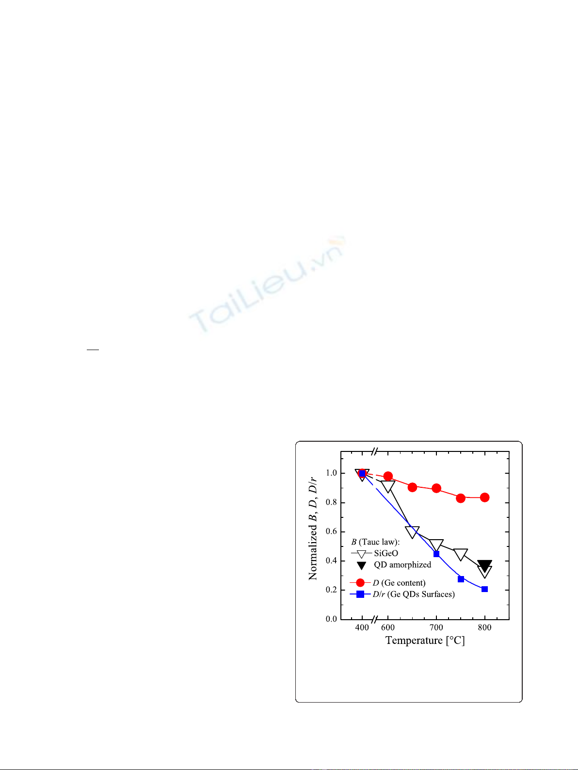
modify the onset of light absorption neither the spec-
trum itself, except that for the disappearance of the
direct resonance peaks as expected because of the lost
crystalline order within the Ge QDs. It should be
remarked that the c-atransition in Si QDs embedded in
SiO
2
actually modifies the absorption by lowering the
optical bandgap of about 0.4 eV [10]. This effect has
been predicted to occur in both Si and Ge QDs by theo-
retical calculations of the electronic bandgap [12,13].
Thus, the data presented in this work evidence a diver-
gence in the behavior of Ge QDs with respect to Si
ones. Moreover, in Ge QDs, the aspectra at 800°C
(both c-ora-Ge QDs) are halved with respect to as-
deposited sample, while the Ge content reduction due
to Ge out-diffusion was measured to be less than 20%.
Thus, annealing at high temperatures clearly induces a
not-negligible fall in the light absorption efficiency of
Ge QDs, while QD structural phase does not affect the
onset of light absorption.
To account for these effects, the Tauc law, describing
ain amorphous semiconductors, has been used [36]:
BE
hv hv g
opt 2,
where hν,B,andE
optg
are the incoming photon
energy, the Tauc constant, and the optical bandgap,
respectively. The photon absorption leads to transitions
between the extended electronic states from the valence
band toward the conduction band, being E
optg
the
energy difference and Bproportional to the convolution
of the density of electronic states (DOS) in the two
energy bands. The Tauc plots, (ahν)
1/12
versus hν,of
selected samples are reported with symbols in Figure 4b,
while lines are the linear fit used to determine Band
E
optg
. For reference, a thin (120 nm) amorphous Ge film
was deposited on quartz, and its Tauc plot (stars) is also
reported with its fit. Tauc plots have a linear slope over
awiderangeofenergy,andtheverygoodagreement
between fits and experimental data justifies the Tauc
approach.
The optical bandgap of a-Ge results 0.8 eV, in good
agreement with the literature [37], while the samples
containing Ge QDs always exhibit an E
optg
of approxi-
mately 1.6 eV (well larger than not-confined Ge), inde-
pendently of the annealing temperature and of the
structural phase (aor c). A similar E
optg
has been
reported in the literature only for one sample containing
Ge QDs in a TiO
2
matrix [23], without variation of
annealing temperature or structural phase. In order to
account for the E
optg
of QDs, quantum confinement
effect can be invoked since the size is well below the
excitonic Bohr radius. In Figure 2, the QD size enlarge-
ment was reported, but it is not accomplished by a
reduction of the E
optg
, as expected if only the confine-
ment rule applies. Such a contrast indicates that the
confinement rule alone cannot account for the mechan-
ism of photon absorption in Ge QDs, or it is masked by
a stronger phenomenon.
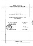
The reduction of awith temperature (Figure 4a) can
be instead ascribed to a significant decreasing of the
Tauc constant (B) as evident from the falling slopes of
fits in Figure 4b. In fact, the Bvalues, normalized to
the as-deposited case, are reported as open triangles in
Figure 5, revealing that after 800°C annealing, the DOS
in Ge QDs involved in the light absorption (proportional
to B) is strongly reduced to about one third, indepen-
dently of the Ge QDs phase (cor a,openorclosedtri-
angles, respectively). If the DOS was related only to the
density of Ge-Ge bonds, the Btrend would decrease
as much as the Ge content in the film (D,circlesin
Figure 5, as measured by RBS and normalized to the as-
deposited case), but this is not the case. Instead, the
photon absorption could be related to Ge bonds near
the QD surfaces. If so, given a fixed amount of clustered
Ge, the Bvalue would be larger the smaller is r.Since
the surface to volume ratio is proportional to 1/rand
thevolumeisproportionaltoD,thetotalareaofthe
surfaces of Ge QDs should decrease as D/r,reportedin
Figure 5 as squares. The patent correlation between B
and D/r trends clearly suggests that the light absorption
in Ge QDs embedded in SiO
2
is strongly influenced by
the surface of Ge QDs. In addition, such an evidence
Figure 5 Tauc constant, Ge content, and the surfaces of Ge
QDs. Comparison between the Tauc constant (B, triangles) as
obtained from Tauc fits, the Ge content (D, circles) as measured by
RBS, and the surfaces of Ge QDs (D/r, squares). All the values have
been normalized to that of the as-deposited sample (color online).
Cosentino et al.Nanoscale Research Letters 2011, 6:135
http://www.nanoscalereslett.com/content/6/1/135
Page 5 of 7


%20--%3e%3cdefs%3e%3cstyle%3e%20.st0%20{%20fill:%20%23fff;%20}%20.st1%20{%20fill:%20%237800fa;%20}%20%3c/style%3e%3c/defs%3e%3cpath%20class='st1'%20d='M117.78,12.18H43.11c2.9,3.47,4.65,7.94,4.65,12.82,0,5.6-2.3,10.66-6.01,14.29h76.02l7.22-13.56-7.22-13.56Z'/%3e%3cg%3e%3cpath%20class='st0'%20d='M53.58,26.17h-.59v-1.46h.59v-4.96h2.83c1.78,0,2.67.94,2.67,2.82v5.76c0,1.87-.89,2.81-2.67,2.81h-2.83v-4.96ZM55.36,21.37v3.34h1.1v1.46h-1.1v3.34h1.01c.61,0,.91-.37.91-1.1v-5.93c0-.74-.3-1.1-.91-1.1h-1.01Z'/%3e%3cpath%20class='st0'%20d='M65.99,31.14h-1.8l-.31-2.07h-2.19l-.31,2.07h-1.64l1.82-11.39h2.62l1.82,11.39ZM65.28,18.04c-.25.46-.51.77-.75.94-.21.15-.47.22-.79.22-.26,0-.57-.07-.92-.22l-.38-.15c-.14-.05-.26-.07-.37-.07-.3,0-.53.18-.71.54l-.91-.68c.25-.46.51-.77.75-.94.21-.14.48-.21.79-.21.26,0,.57.07.92.21l.38.15c.14.05.26.07.37.07.3,0,.53-.18.71-.54l.91.68ZM61.91,27.52h1.73l-.87-5.76-.87,5.76Z'/%3e%3cpath%20class='st0'%20d='M74.53,26.89v1.52c0,1.91-.89,2.86-2.67,2.86s-2.67-.95-2.67-2.86v-5.93c0-1.91.89-2.86,2.67-2.86s2.67.95,2.67,2.86v1.11h-1.69v-1.22c0-.75-.31-1.12-.93-1.12s-.93.37-.93,1.12v6.15c0,.74.31,1.11.93,1.11s.93-.37.93-1.11v-1.63h1.69Z'/%3e%3cpath%20class='st0'%20d='M81.4,31.14h-1.8l-.31-2.07h-2.19l-.31,2.07h-1.64l1.82-11.39h2.62l1.82,11.39ZM75.9,19.2l1.52-1.91h1.71l1.51,1.91h-1.61l-.76-.95-.75.95h-1.61ZM77.32,27.52h1.73l-.87-5.76-.87,5.76ZM83.1,15.99l-1.76,1.91h-1.26l1.17-1.91h1.86Z'/%3e%3cpath%20class='st0'%20d='M84.86,19.75c1.78,0,2.67.94,2.67,2.82v1.48c0,1.87-.89,2.81-2.67,2.81h-.85v4.28h-1.79v-11.39h2.64ZM84.01,21.37v3.86h.85c.58,0,.87-.36.87-1.08v-1.71c0-.71-.29-1.07-.87-1.07h-.85Z'/%3e%3cpath%20class='st0'%20d='M93.51,19.75c1.78,0,2.67.94,2.67,2.82v1.48c0,1.87-.89,2.81-2.67,2.81h-.85v4.28h-1.79v-11.39h2.64ZM92.66,21.37v3.86h.85c.58,0,.87-.36.87-1.08v-1.71c0-.71-.29-1.07-.87-1.07h-.85Z'/%3e%3cpath%20class='st0'%20d='M98.8,31.14h-1.79v-11.39h1.79v4.88h2.03v-4.88h1.83v11.39h-1.83v-4.88h-2.03v4.88Z'/%3e%3cpath%20class='st0'%20d='M105.36,24.55h2.46v1.62h-2.46v3.34h3.09v1.63h-4.88v-11.39h4.88v1.63h-3.09v3.18ZM108.17,17.29l-1.76,1.91h-1.26l1.17-1.91h1.86Z'/%3e%3cpath%20class='st0'%20d='M112.2,19.75c1.78,0,2.67.94,2.67,2.82v1.48c0,1.87-.89,2.81-2.67,2.81h-.85v4.28h-1.79v-11.39h2.64ZM111.35,21.37v3.86h.85c.58,0,.87-.36.87-1.08v-1.71c0-.71-.29-1.07-.87-1.07h-.85Z'/%3e%3c/g%3e%3ccircle%20class='st1'%20cx='25'%20cy='25'%20r='20'/%3e%3cpath%20class='st0'%20d='M32.78,19.27c2.92,0,4.43,2.55,5.28,5.33l.71,2.17c.14.38-.33.75-.71.75h-5.61c.19-.33.24-.71.09-1.08l-.75-2.45c-.43-1.32-.99-2.64-1.79-3.77.75-.57,1.65-.94,2.78-.94h0ZM25,18.38c3.25,0,4.9,2.78,5.89,5.89l.76,2.45c.14.42-.33.8-.8.8h-11.69c-.42,0-.94-.38-.8-.8l.75-2.45c.99-3.11,2.64-5.89,5.89-5.89h0ZM25,11.35c1.74,0,3.11,1.37,3.11,3.11s-1.37,3.11-3.11,3.11-3.11-1.41-3.11-3.11,1.41-3.11,3.11-3.11h0ZM17.27,19.27c1.08,0,1.98.38,2.73.94-.8,1.13-1.37,2.45-1.74,3.77l-.8,2.45c-.14.38-.05.75.09,1.08h-5.56c-.42,0-.9-.38-.75-.75l.71-2.17c.9-2.78,2.41-5.33,5.33-5.33h0ZM17.27,12.91c1.51,0,2.78,1.27,2.78,2.83s-1.27,2.83-2.78,2.83-2.83-1.27-2.83-2.83,1.27-2.83,2.83-2.83h0ZM32.78,12.91c1.56,0,2.78,1.27,2.78,2.83s-1.23,2.83-2.78,2.83-2.83-1.27-2.83-2.83,1.27-2.83,2.83-2.83h0ZM27.07,28.56v.09c0,.57-.24,1.08-.61,1.46h0v.05c-.38.33-.9.57-1.46.57s-1.08-.24-1.46-.61h0c-.38-.38-.61-.9-.61-1.46v-.09h1.41v.09c0,.19.05.38.19.47v.05c.09.09.28.19.47.19s.38-.09.47-.19v-.05c.14-.09.24-.28.24-.47t-.05-.09h1.41ZM30.99,28.56v.09c0,1.65-.66,3.16-1.74,4.24-1.08,1.08-2.59,1.79-4.24,1.79s-3.16-.71-4.24-1.79l-.05-.05c-1.04-1.08-1.7-2.55-1.7-4.2v-.09h1.41v.09c0,1.27.47,2.4,1.27,3.25h.05c.85.85,1.98,1.37,3.25,1.37s2.4-.52,3.25-1.37c.85-.8,1.37-1.98,1.37-3.25v-.09h1.37ZM34.99,28.56v.09c0,2.78-1.13,5.28-2.92,7.07-1.79,1.79-4.29,2.92-7.07,2.92s-5.23-1.13-7.07-2.92c-1.79-1.79-2.92-4.29-2.92-7.07v-.09h1.41v.09c0,2.4.94,4.53,2.5,6.08,1.56,1.56,3.72,2.5,6.08,2.5s4.52-.94,6.08-2.5c1.56-1.56,2.5-3.68,2.5-6.08v-.09h1.41Z'/%3e%3c/svg%3e)