
NANO EXPRESS Open Access
Ultraviolet photodetectors based on ZnO
nanorods-seed layer effect and metal oxide
modifying layer effect
Hai Zhou, Guojia Fang
*
, Nishuang Liu, Xingzhong Zhao
Abstract
Pt/ZnO nanorod (NR) and Pt/modified ZnO NR Schottky barrier ultraviolet (UV) photodetectors (PDs) were prepared
with different seed layers and metal oxide modifying layer materials. In this paper, we discussed the effect of metal
oxide modifying layer on the performance of UV PDs pre- and post-deposition annealing at 300°C, respectively. For
Schottky barrier UV PDs with different seed layers, the MgZnO seed layer-PDs without metal oxide coating showed
bigger responsivity and larger detectivity (D
l
*) than those of PDs with ZnO seed layer, and the reason was
illustrated through energy band theory and the electron transport mechanism. Also the ratio of D
254
*toD
546
* was
calculated above 8 × 10
2
for all PDs, which demonstrated that our PDs showed high selectivity for detecting UV
light with less influence of light with long wavelength.
Introduction
Recently, a one-dimensional (1D) nanomaterial has
attracted a lot of attention both for fundamental research
and potential nano-device applications because of its pecu-
liar characteristics and quantum size effect [1,2]. Among
the various nano-structured materials, due to their direct
and wide energy bandgap (3.37 eV), ZnO nanorods (NRs)
are a promising functional material as potential candidates
for short-wavelength optoelectronics applications such as
nanoscale lasers [3], light-emitting diodes [4], and ultravio-
let (UV) photodetectors (PDs) [5-9]. Although ZnO has
many advantages, the existence of many defects of ZnO
NRs prepared by hydrothermal method [10] may benefit
the formation of ohmic contacts at the electrode/ZnO
NRs interface, which is an obstacle to applications in PDs
due to its slow response and recovery behaviors.
The Schottky barrier plays an important role in improv-
ing the performance of the PDs, and many researchers
have investigated the Schottky contact between ZnO NRs
and metal [11-15], but investigations on effects of metal
oxide coating and seed layer on ZnO NW Schottky PDs
using post-deposition thermal annealing treatment are
scarce. In this study, to investigate the effect of the seed
layer and oxide material on the performance of PDs, a
simple route to gain Schottky barrier by deposition of Pt
electrodes on the top of different oxide material-coated n-
ZnO NRs, which are prepared by hydrothermal process
on different seed layers is introduced. Then, the samples
are treated by thermal annealing process to form Schottky
contacts. In this article, the authors have discussed the
effects of metal oxide-modified layer on the performance
of UV PDs pre- and after post-deposition annealing at
300°C. The investigation of PDs with different seed layers
shows that the MgZnO seed layer-PDs without metal
oxide coating demonstrates bigger responsivity and larger
detectivity than those of PDs with ZnO seed layer, and the
reason has been illustrated through energy band theory
and the electron transport mechanism. Also the ratio of
detectivity (D
l
*, D
254
*toD
546
*) is calculated above 8 × 10
2
for all PDs, which demonstrates that our PDs show high
selectivity for detecting UV light with lesser influence of
light with long wavelength. The attractiveness of this study
is the simplicity of the fabrication process, which could
easily be scaled up, and our results may pave the way for
the application of low-cost ZnO NRs UV PDs.
Experimental methods
The glass substrates were initially cleaned with acetone
in an ultrasonic bath, rinsed with deionized water, and
* Correspondence: gjfang@whu.edu.cn
Department of Electronic Science and Technology and Key Laboratory of
Artificial Micro- and Nano-structures of Ministry of Education, School of
Physics and Technology, Wuhan University, Wuhan 430072, People’s
Republic of China
Zhou et al.Nanoscale Research Letters 2011, 6:147
http://www.nanoscalereslett.com/content/6/1/147
© 2011 Zhou et al; licensee Springer. This is an Open Access article distributed under the terms of the Creative Commons Attribution
License (http://creativecommons.org/licenses/by/2.0), which permits unrestricted use, distribution, and reproduction in any medium,
provided the original work is properly cited.
then blown dry with dry N
2
. Then, a 120-nm ZnO seed
layer was deposited by radio frequency-reactive magne-
tron sputtering at 100°C. Then, ZnO NRs were grown
on ZnO-coated glass substrate by hydrothermal method.
The details of the hydrothermal conditions for obtaining
ZnO NRs have already been reported elsewhere. In
brief, the nutrient solution was an aqueous solution of a
0.05 M zinc nitrate hexahydrate (Zn(NO
3
)
2
·6H
2
O) and
methenamine (C
6
H
12
N
4
). The reaction was kept at
100°C for 2 h, and then, the ZnO NRs flat film was
obtained. Then, to investigate the effect of metal oxide-
modified layer on the performance of UV PDs, MgZnO,
MgO, and Al-doped ZnO were deposited on ZnO NRs
at 100°C by a simple mask plate with radio frequency-
reactive magnetron sputtering followed by deposition of
100-nm Pt. The thickness of the metal oxide layer was
about 50 nm. Finally, for comparison, a few samples
were annealed in air at the temperature of 300°C for
2 h. To investigate the effect of seed layer on the perfor-
mance of UV PDs, MgZnO seed layer-PDs are prepared
without coating oxides, and the experimental conditions
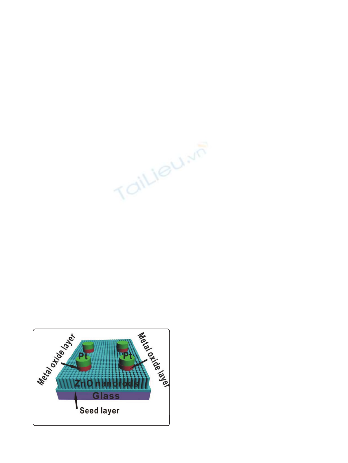
were the same as has been mentioned above. A sche-
matic structure of PD with the sample size of 1 × 1 cm
2
is shown in the inset of Figure 1, and the photon win-
dow area is 1 × 4 mm
2
. The morphology was observed
by Sirion field emission scanning electron microscopy
(Philips XL30). The photosensitivity was performed
using 66984 Xe Arc source (300 W Oriel) and Oriel
Cornerstone TM 260 1/4 m Monochromator. The sam-
ple was under illumination directly (parallel with the
NRs), and the optical power of light was measured by a
UV-enhanced Si detector. All the I-Vcharacteristics
were measured using a Keithley 4200 electrometer.
Results and discussion
In our experiment, the as-prepared ZnO NRs grow verti-
cally and closely packed on the ZnO seed layer, the gap
between ZnO nanowires is very little, and the average dia-
meter and length of these ZnO NRs are around 90-150
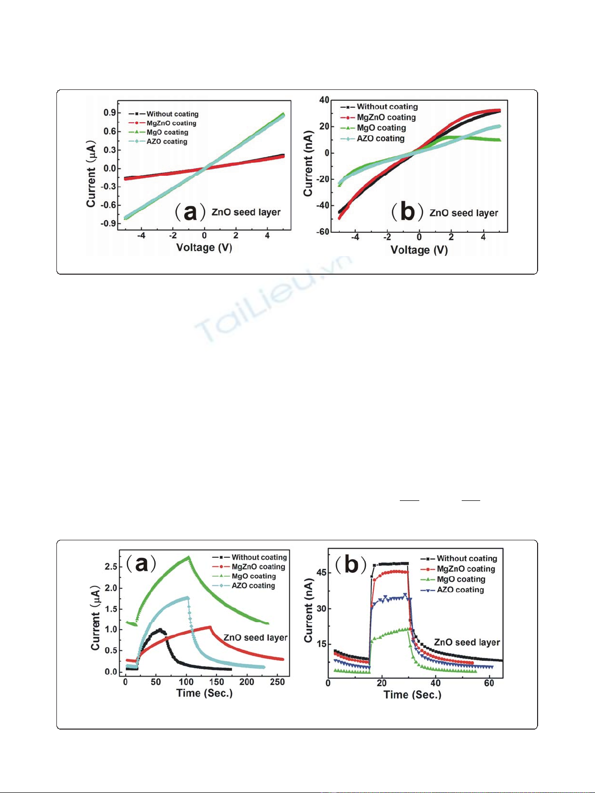
nm and 1.4 μm. The I-Vcurves of the PDs with ZnO seed
layer are shown in Figure 2a. From the curves, the plots of
Ivs. Vare straight lines for ZnO seed layer, showing that
the contacts at the Pt/ZnO NRs or the Pt/metal oxide
interfaces are ohmic. Figure 2b shows the I-Vcurves of
the PDs annealed at 300°C with ZnO seed layer. It can be
seen that when the PDs are annealed at 300°C, the
Schottky contacts are obtained. Also, after the annealing
process, the dark current of PDs decreases greatly. It has
been reported that the as-grown ZnO NRs have large
defect concentration, which can be improved by thermal
annealing [10]. The authors think that the contacts at the
electrode/as-prepared ZnO NRs interface are normally
ohmic, which is due to the existence of many defects, such
as oxygen vacancies or zinc interstitials, resulting in high
carrier density, so that the formation of Schottky contacts
is very hard, even with the contacts between as-prepared
ZnO NRs and electrodes with high work function metals,
such as Au, Ni, and Pt. When ZnO NRs are annealed at
certain temperatures, the defects will be reduced, and the
defect-related carrier density will also decrease, so that the
Schottky contact barrier will be formed.
For PDs, the response and recovery times are a very
important factor for applications. The dependences of
photocurrent on operating time for the PDs with different
oxides under UV light (365 nm) with power density of
16.7 μW/cm
2
atthebiasof2VareshowninFigure3a
(before annealing) and Figure 3b (annealed at 300°C),
respectively. From Figure 3a, under 365-nm UV illumina-
tion, the current of the PDs increases very slowly to reach
saturation, and at turn off of the UV lamp, the current
decreases also slowly. Also it is deduced that the response
time of the PDs is all above 30 s, and the recovery time of
the PDs (the photocurrent decreases 80%) is all above
50 s. For the PDs with different oxide-coating materials,
the devices show enhanced UV response characteristic, but
the response and recovery are all slow. After annealing, all
PDs show fast response and recovery behaviors, and their
response and recovery times are 3 and 4 s, respectively. For
PDs with different oxide coatings, the UV response charac-
teristic gets worse than that of PDs without metal oxide
coating, which shows that the effect of metal oxide coating
for Schottky contact PDs is a negative one.
It is very well known that the metal oxides deposited
at 100°C have some structure defects with high carrier
density, which will benefit the formation of ohmic con-
tacts and electron transport. Hence, the metal oxide, as
an electron transport layer in PDs, can improve the con-
tact resistance between metal and semiconductor.
Therefore, the PDs with metal oxide coating can
enhance photoresponse characteristic before annealing.
After annealing, the structure defects decrease, and the
electrical resistivity of all metal oxides will increase, the
photogenerated electrons will be blocked, and very few
Figure 1 A schematic diagram of PD.
Zhou et al.Nanoscale Research Letters 2011, 6:147
http://www.nanoscalereslett.com/content/6/1/147
Page 2 of 6
can be collected by Pt electrode at forward bias. How-
ever, for PDs without oxide coatings, the contacts at Pt/
ZnO NRs interfaces are improved by annealing process,
and the photogenerated electrons can easily reach to Pt
electrode at forward bias and get high photocurrent, and
PDs without oxide coatings show fast response and
recovery behavior after annealing. Therefore, it is con-
cluded that the PDs without oxide coatings display bet-
ter performance than those with oxide coatings.
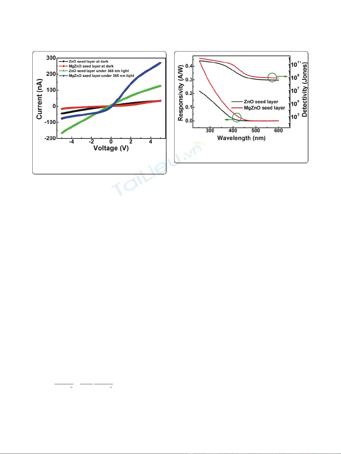
In order to investigate the effect of the seed layer on
the performance of PDs, ZnO NRs are prepared with
two kinds of seed layers (MgZnO and ZnO seed layers).
Herein, high pure ZnO is chosen for the matching of
energy band with that of ZnO NRs. MgZnO is chosen
due to its low carrier density and large band gap (about
4.0 eV). Figure 4 shows the I-Vcurves of the PDs with-
out oxide coating and annealed at 300°C, which demon-
strates the electron transport characteristics of PDs with
different seed layers at dark and under 365-nm UV
light, respectively. From the curves, it can be seen that
the contacts between Pt and ZnO NRs are good
Schottky contacts. At dark, the PD with MgZnO seed
layer has lower dark current than that with ZnO seed
layer, which may be attributed to the lower carrier den-
sity of MgZnO film. Under 365-nm UV light, the cur-
rent of the PD with MgZnO seed layer is higher than
that of the PD with ZnO seed layer at forward bias. The
ratios of photocurrent to dark current RII
Ph D
/
calcu-
lated for the PDs with MgZnO and ZnO seed layer at
5 V are 3.9 and 8.2, respectively.
For Schottky barrier PDs, the actual barrier height at
the electrode/semiconductor interface is an important
part of the PDs under investigation. The Schottky bar-
rier height can be determined using I-Vmeasurements
as per Equation (1) [13]
IAAT q
KT
qV
nKT
*exp exp
21
B(1)
Figure 2 The I-Vcurves of the PDs with different metal oxide coatings.(a) Before annealing; (b) after annealing at 300°C.
Figure 3 The dependences of photocurrents on operating time for PDs with different metal oxide coatings under UV light (365 nm)
with power density of 16.7 μW/cm
2
at the bias of 2 V.(a) Before annealing; (b) after annealing at 300°C.
Zhou et al.Nanoscale Research Letters 2011, 6:147
http://www.nanoscalereslett.com/content/6/1/147
Page 3 of 6
where nis the ideal factor, Kis the Boltzmann’scon-
stant, Tis the absolute temperature, F
B
is the barrier
height, Ais the Schottky contact area, and A* is the
effective Richardson coefficient constant. By means of
forward biased I-Vmeasurements and Equation (1), it
can be deduced that for the PDs with ZnO and MgZnO
seed layer, Schottky barrier heights F
B
at the Pt/ZnO
NRs interface are, respectively, about 0.768 and 0.796
eV at dark and the respective F
B
values are about 0.738
and 0.734 eV under 365-nm light. From above, it can be
seen that F
B
decreases under 365-nm light, and it
decreases by 0.03 and 0.062 eV for the PDs with ZnO
and MgZnO seed layer, respectively. The decrease of F
B
for the PDs with MgZnO seed layer is two times that
for the PDs with ZnO seed layer, which illustrates that
the larger increase of photocurrent will result in the lar-
ger decrease of F
B
.
Theresponsivity(R) is an important parameter to
reflect the performance of PDs, and so the spectral R
curves obtained from non-oxide-coated PDs annealed at
300°C with different seed layer under the forward biases
of 2 V are presented in Figure 5. From these spectra, it
can be seen that the responsivity of the PDs with
MgZnO seed layer is higher than that of the PDs with
ZnO seed layer and reaches to as high as 0.44 A/W at
254 nm, which is double that of PDs with ZnO seed
layer (0.22 A/W). The detectivity is also calculated,
which is given by the following [16]:
DR
qJ
J
LqJ
*
() ()
2
1
2
1
2
1
2
d
ph
light d
(2)
where Ris the responsivity of the photodiode, J
d
is the
dark current, J
ph
is the photocurrent density, and L
light
is the light intensity. Detectivity is calculated and also
plotted in Figure 5. From the curves of the detectivity of
PDs, it can be noted that the Schottky barrier PDs
exhibited spectral response mainly in the range from
250 to 400 nm, with the detectivity above 10
11
Jones (1
Jones = 1 cmHz
1/2
/W), and the detectivity of the PDs
with MgZnO seed layer is higher than that of the PDs
with ZnO seed layer. At the wavelength above 400 nm,
the PDs show little detectivity, and the detectivity
decreases with the increase of the wavelength. The ratio
of D
254
*toD
546
* is above 8 × 10
2
, which shows that the
PDs have high selectivity for detecting UV light with
less influence of light with long wavelength.
In order to explore the enhanced performance of PDs
with MgZnO seed layer, carrier transport processes in
the ZnO NRs PDs under forward bias are illustrated in
Figure 6a. In the dark, oxygen is adsorbed at the surface
of the NRs to form a chemically adsorbed surface state.
Under UV illumination, electron-hole pairs are gener-
ated when photon energy exceeds the energy band gap
(hυ>E
g
). Photogenerated holes move to the surface of
ZnO NRs and the adsorbed oxygen is photodesorbed,
and unpaired electrons in the NRs migrate to the elec-
trodes at a bias voltage and contribute to the photocur-
rent [6,12]. From Figure 6a, it can be seen that the
photogenerated electrons, generated from the surface of
ZnO NRs, move to the MgZnO layer at first, and then
move from MgZnO to ZnO NRs, which are underneath
the electrode, and finally reach to the electrode. Owing
to the high contact resistance among NRs, a few photo-
generated electrons may pass from NRs and contribute
to the photocurrent. In Figure 6b, the Schottky barrier
height F
B
is calculated using forward- or reverse-biased
I-Vmeasurements and Equation (1). From Figure 6b, it
can be seen that at dark, the barrier height between
ZnO NRs and MgZnO (ΔE
c1
) is the same as that
Figure 4 The I-Vcurves of the PDs based on ZnO or MgZnO
seed layer without metal oxide coating measured at dark and
under 365 nm UV light.
Figure 5 The spectral responsivity and detectivity curves of
PDs without metal oxide coating under the forward biases of
2V.
Zhou et al.Nanoscale Research Letters 2011, 6:147
http://www.nanoscalereslett.com/content/6/1/147
Page 4 of 6
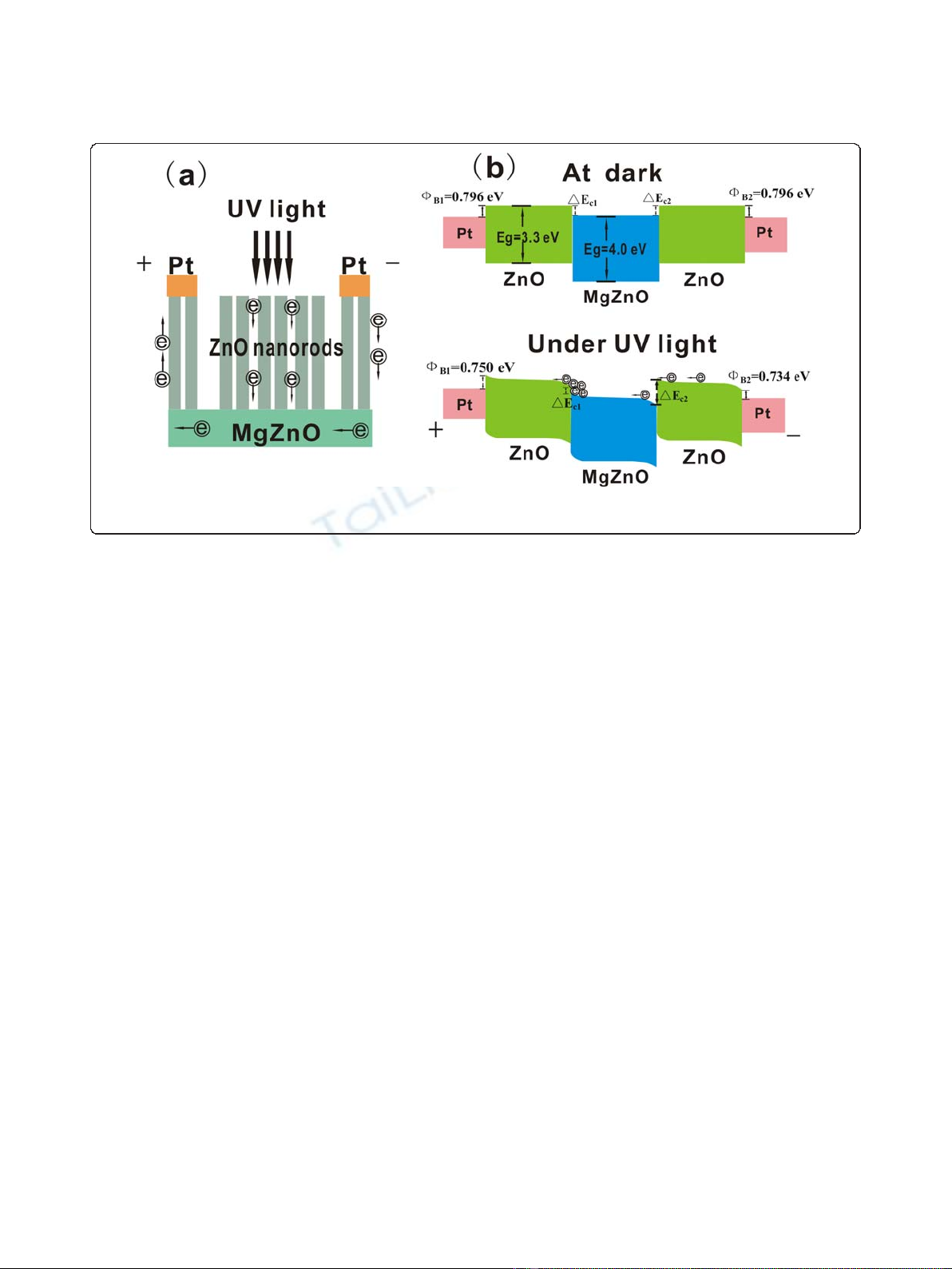
between MgZnO and ZnO NRs (ΔE
c2
). Under UV illu-
mination, ΔE
c2
gets larger, and ΔE
c1
gets smaller at for-
ward bias, which benefits the photogenerated electrons
moving from ZnO NRs to MgZnO. Owing to existence
of the small ΔE
c1
, the photogenerated electrons will col-
lect together at the ZnO NRs/MgZnO interface, and
then the two-dimensional electron gas (2DEG) will form
[17]. The 2DEG will decrease the transverse resistances
between the interface strongly [18], and then the photo-
generated electrons may reach easily to Pt electrode.
Therefore, compared with the PDs with ZnO seed layer,
the PDs with MgZnO seed layer can realize bigger
responsivity and higher detectivity.
Conclusions
In conclusion, Schottky barrier PDs based on ZnO NRs
were prepared by varying seed layers and metal oxide-
coating materials. Before annealing, PDs coated with
metal oxide materials showed enhanced photoresponse
compared to that without coatings. However, after
annealing treatment, the metal oxides will block photo-
generated electrons to electrodes and reduce photocur-
rent. Also, after annealing at 300°C, contacts at the
electrode/ZnO NRs or electrode/oxide interface were
Schottky type, and the performance of the PDs has
improved with the great decrease of response and recov-
ery times. For different seed layer-PDs without oxide
coating, the PDs with MgZnO seed layer showed bigger
responsivity and lager detectivity than those of PDs
with ZnO seed layer, and the ratio of D
254
*toD
546
* was
above 8 × 10
2
for all PDs. The results may provide
a simple route to obtain low-cost high performance
UV PDs.
Abbreviations
NR: nanorod; PDs: photodetectors; UV: ultraviolet.
Acknowledgements
This study was partially supported by the National High Technology
Research and Development Program of China (2009AA03Z219), the National
Basic Research Program (2011CB933300) of China, the National Natural
Science Foundation of China (11074194), and the Special Fund of Ministry of
Education for Doctor’s Conferment Post under grant No. 20070486015.
Authors’contributions
All authors contributed equally and read and approved the final manuscript.
Competing interests
The authors declare that they have no competing interests.
Received: 5 October 2010 Accepted: 15 February 2011
Published: 15 February 2011
References
1. Huang MH, Mao S, Feick H, Yan H, Wu Y, Kind H, Weber E, Russo R, Yang P:
Room-temperature ultraviolet nanowire nanolasers. Science 2001,
292:1897.
2. Huang MH, Wu Y, Feick H, Tran N, Weber E, Yang P: Catalytic growth of
zinc oxide nanowires by vapor transport. Adv Mater 2001, 13:113.
3. Yang P, Yan H, Mao S, Russo R, Johnson J, Saykally R, Morris N, Pham J,
He R, Choi HJ: Controlled growth of ZnO nanowires and their optical
properties. Adv Funct Mater 2002, 12:323.
4. Liu CH, Zapien JA, Yao Y, Meng XM, Lee CS, Fan SS, Lifshitz SS, Lee SS:
High - Density, Ordered Ultraviolet Light - Emitting ZnO Nanowire
Arrays. Adv Mater 2003, 15:838-841.
5. Kind H, Yan H, Messer B, Law M, Yang P: Nanowire ultraviolet
photodetectors and optical switches. Adv Mater 2002, 14:158-160.
6. Soci C, Zhang A, Xiang B, Dayeh SA, Aplin DPR, Park J, Bao XY, Lo YH,
Wang D: ZnO nanowire UV photodetectors with high internal gain. Nano
Lett 2007, 7:1003-1009.
Figure 6 Carrier transport processes in the ZnO NRs PDs.(a) Photogenerated electron transport route under UV illumination. (b) Schematic
energy level diagrams of the PD with MgZnO seed layer at dark and under UV illumination, respectively.
Zhou et al.Nanoscale Research Letters 2011, 6:147
http://www.nanoscalereslett.com/content/6/1/147
Page 5 of 6


%20--%3e%3cdefs%3e%3cstyle%3e%20.st0%20{%20fill:%20%23fff;%20}%20.st1%20{%20fill:%20%237800fa;%20}%20%3c/style%3e%3c/defs%3e%3cpath%20class='st1'%20d='M117.78,12.18H43.11c2.9,3.47,4.65,7.94,4.65,12.82,0,5.6-2.3,10.66-6.01,14.29h76.02l7.22-13.56-7.22-13.56Z'/%3e%3cg%3e%3cpath%20class='st0'%20d='M53.58,26.17h-.59v-1.46h.59v-4.96h2.83c1.78,0,2.67.94,2.67,2.82v5.76c0,1.87-.89,2.81-2.67,2.81h-2.83v-4.96ZM55.36,21.37v3.34h1.1v1.46h-1.1v3.34h1.01c.61,0,.91-.37.91-1.1v-5.93c0-.74-.3-1.1-.91-1.1h-1.01Z'/%3e%3cpath%20class='st0'%20d='M65.99,31.14h-1.8l-.31-2.07h-2.19l-.31,2.07h-1.64l1.82-11.39h2.62l1.82,11.39ZM65.28,18.04c-.25.46-.51.77-.75.94-.21.15-.47.22-.79.22-.26,0-.57-.07-.92-.22l-.38-.15c-.14-.05-.26-.07-.37-.07-.3,0-.53.18-.71.54l-.91-.68c.25-.46.51-.77.75-.94.21-.14.48-.21.79-.21.26,0,.57.07.92.21l.38.15c.14.05.26.07.37.07.3,0,.53-.18.71-.54l.91.68ZM61.91,27.52h1.73l-.87-5.76-.87,5.76Z'/%3e%3cpath%20class='st0'%20d='M74.53,26.89v1.52c0,1.91-.89,2.86-2.67,2.86s-2.67-.95-2.67-2.86v-5.93c0-1.91.89-2.86,2.67-2.86s2.67.95,2.67,2.86v1.11h-1.69v-1.22c0-.75-.31-1.12-.93-1.12s-.93.37-.93,1.12v6.15c0,.74.31,1.11.93,1.11s.93-.37.93-1.11v-1.63h1.69Z'/%3e%3cpath%20class='st0'%20d='M81.4,31.14h-1.8l-.31-2.07h-2.19l-.31,2.07h-1.64l1.82-11.39h2.62l1.82,11.39ZM75.9,19.2l1.52-1.91h1.71l1.51,1.91h-1.61l-.76-.95-.75.95h-1.61ZM77.32,27.52h1.73l-.87-5.76-.87,5.76ZM83.1,15.99l-1.76,1.91h-1.26l1.17-1.91h1.86Z'/%3e%3cpath%20class='st0'%20d='M84.86,19.75c1.78,0,2.67.94,2.67,2.82v1.48c0,1.87-.89,2.81-2.67,2.81h-.85v4.28h-1.79v-11.39h2.64ZM84.01,21.37v3.86h.85c.58,0,.87-.36.87-1.08v-1.71c0-.71-.29-1.07-.87-1.07h-.85Z'/%3e%3cpath%20class='st0'%20d='M93.51,19.75c1.78,0,2.67.94,2.67,2.82v1.48c0,1.87-.89,2.81-2.67,2.81h-.85v4.28h-1.79v-11.39h2.64ZM92.66,21.37v3.86h.85c.58,0,.87-.36.87-1.08v-1.71c0-.71-.29-1.07-.87-1.07h-.85Z'/%3e%3cpath%20class='st0'%20d='M98.8,31.14h-1.79v-11.39h1.79v4.88h2.03v-4.88h1.83v11.39h-1.83v-4.88h-2.03v4.88Z'/%3e%3cpath%20class='st0'%20d='M105.36,24.55h2.46v1.62h-2.46v3.34h3.09v1.63h-4.88v-11.39h4.88v1.63h-3.09v3.18ZM108.17,17.29l-1.76,1.91h-1.26l1.17-1.91h1.86Z'/%3e%3cpath%20class='st0'%20d='M112.2,19.75c1.78,0,2.67.94,2.67,2.82v1.48c0,1.87-.89,2.81-2.67,2.81h-.85v4.28h-1.79v-11.39h2.64ZM111.35,21.37v3.86h.85c.58,0,.87-.36.87-1.08v-1.71c0-.71-.29-1.07-.87-1.07h-.85Z'/%3e%3c/g%3e%3ccircle%20class='st1'%20cx='25'%20cy='25'%20r='20'/%3e%3cpath%20class='st0'%20d='M32.78,19.27c2.92,0,4.43,2.55,5.28,5.33l.71,2.17c.14.38-.33.75-.71.75h-5.61c.19-.33.24-.71.09-1.08l-.75-2.45c-.43-1.32-.99-2.64-1.79-3.77.75-.57,1.65-.94,2.78-.94h0ZM25,18.38c3.25,0,4.9,2.78,5.89,5.89l.76,2.45c.14.42-.33.8-.8.8h-11.69c-.42,0-.94-.38-.8-.8l.75-2.45c.99-3.11,2.64-5.89,5.89-5.89h0ZM25,11.35c1.74,0,3.11,1.37,3.11,3.11s-1.37,3.11-3.11,3.11-3.11-1.41-3.11-3.11,1.41-3.11,3.11-3.11h0ZM17.27,19.27c1.08,0,1.98.38,2.73.94-.8,1.13-1.37,2.45-1.74,3.77l-.8,2.45c-.14.38-.05.75.09,1.08h-5.56c-.42,0-.9-.38-.75-.75l.71-2.17c.9-2.78,2.41-5.33,5.33-5.33h0ZM17.27,12.91c1.51,0,2.78,1.27,2.78,2.83s-1.27,2.83-2.78,2.83-2.83-1.27-2.83-2.83,1.27-2.83,2.83-2.83h0ZM32.78,12.91c1.56,0,2.78,1.27,2.78,2.83s-1.23,2.83-2.78,2.83-2.83-1.27-2.83-2.83,1.27-2.83,2.83-2.83h0ZM27.07,28.56v.09c0,.57-.24,1.08-.61,1.46h0v.05c-.38.33-.9.57-1.46.57s-1.08-.24-1.46-.61h0c-.38-.38-.61-.9-.61-1.46v-.09h1.41v.09c0,.19.05.38.19.47v.05c.09.09.28.19.47.19s.38-.09.47-.19v-.05c.14-.09.24-.28.24-.47t-.05-.09h1.41ZM30.99,28.56v.09c0,1.65-.66,3.16-1.74,4.24-1.08,1.08-2.59,1.79-4.24,1.79s-3.16-.71-4.24-1.79l-.05-.05c-1.04-1.08-1.7-2.55-1.7-4.2v-.09h1.41v.09c0,1.27.47,2.4,1.27,3.25h.05c.85.85,1.98,1.37,3.25,1.37s2.4-.52,3.25-1.37c.85-.8,1.37-1.98,1.37-3.25v-.09h1.37ZM34.99,28.56v.09c0,2.78-1.13,5.28-2.92,7.07-1.79,1.79-4.29,2.92-7.07,2.92s-5.23-1.13-7.07-2.92c-1.79-1.79-2.92-4.29-2.92-7.07v-.09h1.41v.09c0,2.4.94,4.53,2.5,6.08,1.56,1.56,3.72,2.5,6.08,2.5s4.52-.94,6.08-2.5c1.56-1.56,2.5-3.68,2.5-6.08v-.09h1.41Z'/%3e%3c/svg%3e)