
NANO EXPRESS Open Access
Effect of thermal treatment on the growth,
structure and luminescence of nitride-passivated
silicon nanoclusters
Patrick RJ Wilson
1*
, Tyler Roschuk
1
, Kayne Dunn
1
, Elise N Normand
2
, Evgueni Chelomentsev
1
,
Othman HY Zalloum
1
, Jacek Wojcik
1
, Peter Mascher
1*
Abstract
Silicon nanoclusters (Si-ncs) embedded in silicon nitride films have been studied to determine the effects that
deposition and processing parameters have on their growth, luminescent properties, and electronic structure.
Luminescence was observed from Si-ncs formed in silicon-rich silicon nitride films with a broad range of
compositions and grown using three different types of chemical vapour deposition systems. Photoluminescence
(PL) experiments revealed broad, tunable emissions with peaks ranging from the near-infrared across the full visible
spectrum. The emission energy was highly dependent on the film composition and changed only slightly with
annealing temperature and time, which primarily affected the emission intensity. The PL spectra from films
annealed for duration of times ranging from 2 s to 2 h at 600 and 800°C indicated a fast initial formation and
growth of nanoclusters in the first few seconds of annealing followed by a slow, but steady growth as annealing
time was further increased. X-ray absorption near edge structure at the Si K- and L
3,2
-edges exhibited composition-
dependent phase separation and structural re-ordering of the Si-ncs and silicon nitride host matrix under different
post-deposition annealing conditions and generally supported the trends observed in the PL spectra.
Introduction
Quantum confinement effects have been found to
improve the efficiency of radiative recombination in sili-
con [1]. In accordance with Heisenberg’s uncertainty
principle, the spatial confinement of the charge carriers
induces a spread in their momenta, allowing for quasi-
direct radiative transitions to occur in an indirect band-
gap semiconductor. Utilizing these quantum confine-
ment effects, efficient light emission has been achieved
from silicon nanoclusters (Si-ncs) formed in a dielectric
host matrix. While the properties of this luminescence
have been observed to depend on the size of the Si-ncs,
difficulties arise in the understanding of these materials
from the effects related to the Si-nc/dielectric interface,
as well as from the specific physical properties of the
dielectric matrix. This situation is further compounded
by fabrication-specific issues, where the use of different
deposition systems or source gases for the fabrication of
Si-nc-containing thin films can alter the observed opti-
cal behaviour of the materials, requiring continued
research to gain a better understanding of this materials
system [2,3].
Forming Si-ncs in a silicon nitride host matrix offers
several key advantages over silicon oxide, which was the
focus of many early studies [4-9]. Silicon nitride is a
promising host matrix candidate since it is a structurally
stable dielectric commonly used in microelectronic fab-
rication processes. Favourable electrical properties
resulting from the lower tunnelling barriers allow for
better transport of electronsandholesintoSi-ncs
formed in silicon nitride, making these films better sui-
ted for electroluminescent device applications [10]. In
addition, Si-ncs coordinated with oxygen atoms are sub-
ject to charge trapping related to double-bonds between
silicon and oxygen at the interface, which effectively
limits the emission from such Si-ncs to energies less
than approximately 2 eV, regardless of Si-nc dimensions
[11]. Since Si-ncs coordinated with nitrogen atoms do
* Correspondence: wilsonpr@mcmaster.ca; mascher@mcmaster.ca
1
Department of Engineering Physics and Centre for Emerging Device
Technologies, McMaster University, 1280 Main Street West, Hamilton, Ontario
L8S4L7, Canada
Full list of author information is available at the end of the article
Wilson et al.Nanoscale Research Letters 2011, 6:168
http://www.nanoscalereslett.com/content/6/1/168
© 2011 Wilson et al; licensee Springer. This is an Open Access article distributed under the terms of the Creative Commons Attribution
License (http://creativecommons.org/licenses/by/2.0), which permits unrestricted use, distribution, and reproduction in any medium,
provided the original work is properly cited.

not exhibit the same limitation, emission has been
demonstrated to occur at energies across the entire visi-
ble spectrum [10,12,13]. The process of forming Si-ncs
in silicon nitride is also more favourable due to much
lower annealing temperature requirements for bright
luminescence compared to silicon oxide films where
temperatures must typically exceed 1000°C [14]. In fact,
even before annealing, silicon-rich silicon nitride (SRSN)
films grown by plasma-enhanced chemical vapour
deposition (PECVD) can exhibit efficient luminescence.
However, the formation of Si-ncs in SRSN films has
been found to occur in a more complex fashion, with
formation of both amorphous and crystalline clusters
being reported and a strong dependence on both
deposition and processing conditions [10,15-17].
In this article, Si-ncs formed in SRSN films deposited
with varied compositions using three different chemical
vapour deposition (CVD)-based systems are compared
and discussed: plasma-enhanced CVD (PECVD), induc-
tively coupled plasma CVD (ICP CVD), and electron
cyclotron resonance PECVD (ECR PECVD). Results
from these studies have been previously reported in two
conference proceedings [18,19]. Most studies to date
have employed isochronal annealing steps after deposi-
tion to induce diffusion of excess silicon to nucleation
sites. Conventionally, this has been done using a quartz
tube furnace with an ambient gas of N
2
or N
2
+5%H
2
(i.e. forming gas) over 60 min. For consistency, this
approach has been taken to provide a good comparison
amongst the three deposition systems studied. However,
whilst this provides for good comparison amongst the
results of various studies, to date there has not been an
in-depth isothermal study wherein the annealing is per-
formed over a large time scale ranging from seconds to
hours. To address this gap in reported data, in this
study, SRSN thin films have been annealed for times
ranging from 2 s to 2 h using rapid thermal annealing
to provide a basis for investigating the growth process
and thermal evolution of thesefilmsaswellasdeter-
mining the flexibility of the processing conditions over
which such a film could be incorporated into a larger
device design.
Experimental details
In comparing the three CVD systems, SRSN thin films
were deposited on n-type (100) Si substrates. The sam-
ple compositions were controlled through the variation
of the deposition gas flow rates, adjusting the nitrogen
source rate while keeping the silicon source rate con-
stant. Unless otherwise stated, all depositions were per-
formed with a substrate heater temperature of 300°C,
and the system-specific data for the silicon and nitrogen
source gases, radio frequency (RF) power for PECVD
and ICP CVD, or microwave (MW) power for ECR
PECVD, film thickness, and deposition rate are all listed
in Table 1. Post-deposition, the samples were subjected
to thermal annealing in a quartz tube furnace for 60
min under either flowing N
2
or N
2
+5%H
2
. The char-
acteristics of the Si-ncs are strongly dependent on both
deposition and processing parameters, as evidenced by
variations in their measured luminescent properties and
electronic structure. The films studied in the isothermal
annealing experiments were deposited by the ECR
PECVD system using similar parameters as employed in
the system comparison, except that the films in this case
were grown to be approximately 3000 Å thick and were
deposited using a substrate heater temperature of 350°C
(unless otherwise stated). The higher temperature was
used since this was generally found to produce SRSN
films with increased photoluminescence (PL) intensity
for this particular system. For better temporal accuracy,
the post-deposition annealing was performed using a
Qualiflow Jipelec Jetfirst 100 rapid thermal processor
(RTP) rather than a quartz tube furnace. The isothermal
study was performed using temperatures of 600 and
800°C with a ramp rate of 25°C/s under flowing N
2
gas
for times ranging from 2 to 7200 s. The emission spec-
tra of the films were measured via room temperature
ultraviolet-excited PL using a 17 mW HeCd laser emit-
ting at 325 nm. The complete details of our PL setup
have been described elsewhere [20]. Film compositions
were measured using Rutherford backscattering spectro-
metry (RBS) conducted in the Tandetron Accelerator
Laboratory at the University of Western Ontario. Finally,
X-ray absorption near edge structure (XANES) experi-
ments were performed to obtain information on the
electronic structure of the films at the Si K- and L
3,2
-
edges. The XANES measurements were conducted on
the high resolution spherical grating monochromator
(SGM) [21] and variable line spacing plane grating
monochromator (VLS PGM) [22] beamlines at the
Canadian Light Source synchrotron facility. In these
experiments, both the total electron yield (TEY) and
total fluorescence yield (FLY) were measured
Table 1 System specific details for SRSN thin film depositions
CVD system Si source gas N source gas RF/MW power (W) Film thickness (Å) Deposition rate (Å/min)
PECVD 5% SiH
4
/Ar NH
3
50 2200-2600 110-130
ICP CVD 30% SiH
4
/Ar N
2
300 2400-3000 26-30
ECR PECVD 30% SiH
4
/Ar 10% N
2
/Ar 500 800-1200 53-60
Wilson et al.Nanoscale Research Letters 2011, 6:168
http://www.nanoscalereslett.com/content/6/1/168
Page 2 of 12
simultaneously, normalized to the incident X-ray inten-
sity (I
0
). These yields provide information over different
depths within the sample because of the relative mean
free paths of secondary electrons and fluorescence
photons at the absorption edges probed. Information on
the bulk of the film was provided by the TEY spectra at
the Si K-edge and the FLY spectra at the Si L
3,2
-edge.
Results and discussion
Sample composition
The films produced by each of the three deposition sys-
tems for the isochronal annealing experiments covered a
broad range of compositions from stoichiometric Si
3
N
4
to 14 at.% excess silicon content (Si
ex
) relative to stoi-
chiometry. Here, the excess silicon content for substoi-
chiometric silicon nitride films with composition SiN
x
has been defined as:
Si
ex
=Si
at.%
/(Si
at.%
+N
at.%
) - 3/7 = (1 + x)
-1
- 3/7.
Film compositions were determined by fitting experi-
mental RBS data from the as-deposited (AD) films with
simulated spectra using the SIMNRA software package
[23] and all quoted percentagesinthisstudyreferto
atomic percentages derived from these measurements.
Owing to the inherently poor sensitivity of RBS in mea-
suring lower atomic number elements such as nitrogen,
the values obtained from the fits have been rounded to
the nearest percent, and values measured below 0.5%
have been labelled as <1% to account for the uncertainty
in the data. The films used in the isothermal annealing
experiments were measured to be moderately silicon-
rich, having excess silicon contents of 2-3%. Of these
films, the one used to study the Si K-edge XANES was
deposited at a slightly lower substrate temperature of
300°C, which could have a minor effect on the film’s
properties. However, for the purposes of this study, the
compositions of these films were similar enough to
draw qualitative comparisons between the trends
observed in the PL and XANES spectra obtained from
the different samples.
Isochronal comparison of deposition systems
The luminescent properties of the various films were
analysed through their room temperature ultraviolet-
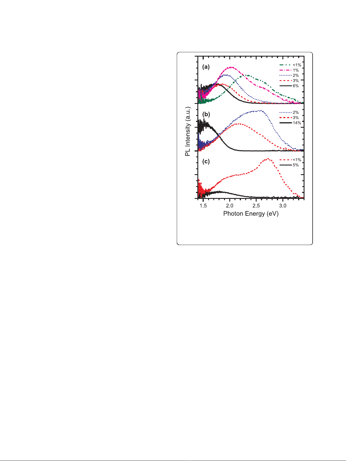
excited PL spectra. Figure 1 compares the PL spectra
from the AD samples from the three systems. Note that
the ECR PECVD film with 2% excess silicon content
depicted in this figure was grown using a slightly higher
substrate heater temperature of 350°C, which may have
resulted in higher emission intensity than a film with
similar composition deposited at 300°C. Despite the dif-
ferences in deposition conditions between the systems,
similar trends can be observed. Each system produces
AD films exhibiting bright PL with emission energies
that can be controlled through the full range of the visi-
ble and into the near-infrared portion of the electromag-
netic spectrum by increasing the excess silicon content
in the film. This correlates well with expected quantum
confinement effects as Si-ncs increase in size. However,
for each system, the emission occurs across a broad
range of energies and appearstooriginatefromacom-
bination of quantum confinement effects and defect
levels, which have peaks at approximately constant ener-
gies independent of the film composition. These defect-
related peaks are most prominent in films with low
excess silicon content, in which smaller Si-ncs form. As
the dimensions of the Si-ncs are reduced, the defect
levels become excited and emission through these levels
becomes more dominant. The fact that significant PL
intensity is observed in the AD films indicates that Si-
ncs are formed within SRSN films without the assistance
of annealing. This is different from what occurs in sili-
con-rich silicon oxide (SRSO) films where cluster forma-
tion and resulting luminescence occur only after high
temperature annealing [14]. The PL intensity of the
SRSN films in this study has been qualitatively described
as ‘bright’, which is a rather arbitrary term. Since quan-
titative measurements of emission intensity have yet to
be performed, the term bright is qualified here as PL
Figure 1 PL spectra for as-deposited SRSN films grown by (a)
PECVD, (b) ECR PECVD, and (c) ICP CVD with their respective
excess silicon contents specified in the legend. As excess silicon
content increases, emission shifts to lower energies.
Wilson et al.Nanoscale Research Letters 2011, 6:168
http://www.nanoscalereslett.com/content/6/1/168
Page 3 of 12
that is easily visible under typical room lighting
conditions.
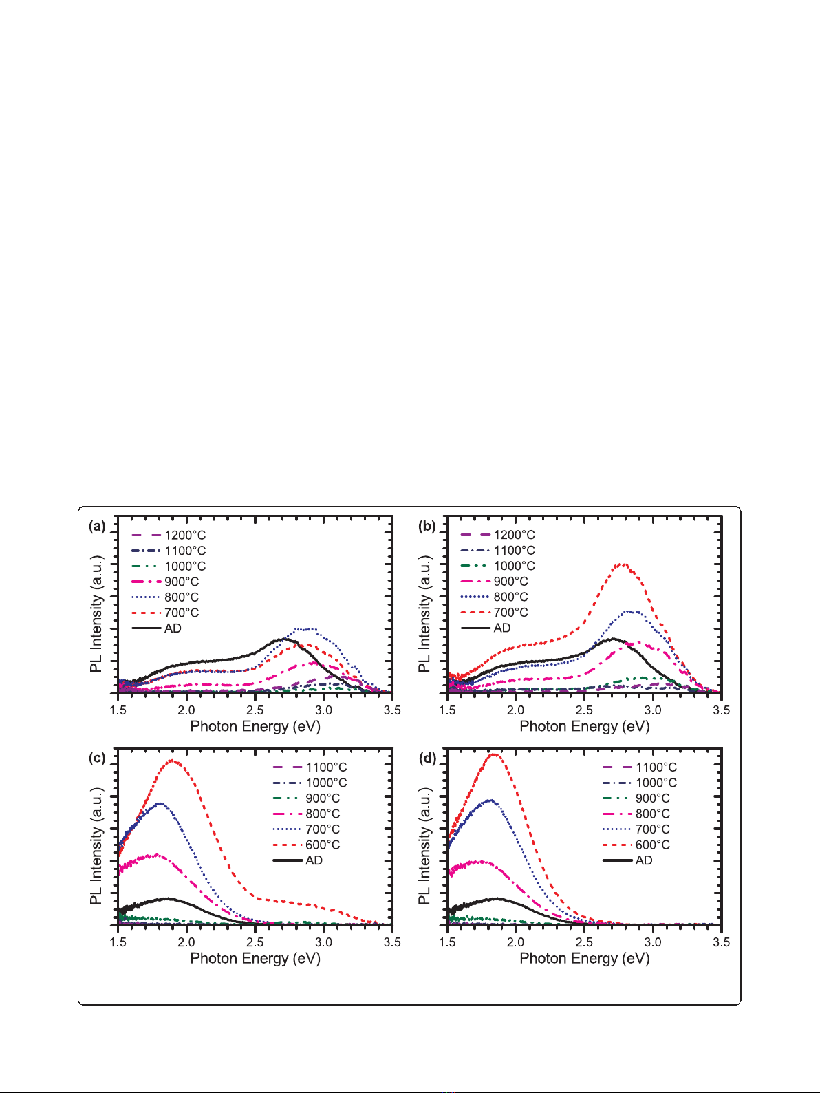
The effects of annealing a PECVD film with moder-
ately high excess silicon content and an ICP CVD film
with low excess silicon content using different ambient
gases are compared in Figure 2. In general, the emission
spectra for samples with higher excess silicon content
tend to red-shift slightly as the annealing temperature is
increased, whereas lower excess silicon content samples
exhibit a slight blue-shift. In samples containing inter-
mediate levels of excess silicon content, the PL peaks
have also been observed to blue-shift relative to the AD
spectra at low temperatures and red-shift as the anneal-
ing temperature is further increased. There appear to be
at least two competing mechanisms in the Si-nc growth
dynamics related to the growth of existing Si-ncs due to
diffusion of silicon atoms in the film and the formation
and subsequent growth of new Si-ncs at nucleation
sites. The red-shifting resulting from Si-nc growth is
much smaller than that observed in SRSO films, but this
can be explained by the more diffusion-inhibiting struc-
ture of the silicon nitride matrix relative to the silicon
oxide matrix [24]. It is also possible that energy may be
transferred between smaller and larger Si-ncs, which
affects the observed PL spectra. In all of the samples,
the most intense emission consistently occurred when
annealing was performed at 800°C or below, with peak
intensities being observed at lower temperatures for
higher silicon content samples. The reason for the decay
in PL intensity at higher temperatures is unknown at
this time since (a) Si-ncs are still present in TEM
images (not shown) and X-ray absorption spectra of
these films and (b) the Si-ncs have not grown beyond
the quantum confinement regime because of the inhibi-
tive nature of the nitride matrix. As the decay in lumi-
nescence does not appear to relate to structural changes
in the Si-nc, this suggests that it results from changes in
the host nitride matrix or with the interface passivation.
Such effects could arise from the strain induced on the
Si-ncs by the nitride matrix or a re-ordering of the
nitride matrix structure at the Si-nc interface such that
non-radiative recombination pathways become available.
However, further investigation is required to accurately
attribute the source of this phenomenon.
Figure 2 PL spectra for films annealed for 60 min in a quartz tube furnace. Shown are an ICP CVD film (Si
ex
< 1%) annealed in (a) N
2
,(b)
N
2
+5%H
2
and a PECVD film (Si
ex
= 3%) annealed in (c) N
2
, and (d) N
2
+5%H
2
.
Wilson et al.Nanoscale Research Letters 2011, 6:168
http://www.nanoscalereslett.com/content/6/1/168
Page 4 of 12
Hydrogen passivation of dangling bonds at the Si-nc
interfaceisalsoobservedtoplayasignificantrolein
improving the PL efficiency. The use of N
2
+5%H
2
rather than pure N
2
as an ambient gas in the annealing
process significantly improves the emission intensity in
the ICP CVD- and ECR PECVD-deposited films. This
enhancement is not observed in the PECVD-deposited
films, which may be because this system uses NH
3
as a
nitrogen source. Higher concentrations of hydrogen may
remain in the film after dissociating from the NH
3
gas
molecules during the CVD reaction process. Having
increased levels of hydrogen in the AD PECVD films
could be very beneficial when considering incorporating
these types of luminescent films into a larger scale design
process, such as for electroluminescent and integrated
circuit device processing, provided it does not reduce the
quality of the film through increased porosity or the
effects of out-gassing. Low temperature rapid thermal
annealing is preferable in such cases due to the shorter
timescale and reduced thermal budget, providing better
compatibility with other materials, structures, or pro-
cesses. Lower temperatures with shorter anneals become
particularly important for avoiding the diffusion of metals
from contacts, and potentially reducing the number of
design steps required compared to the typically longer
quartz tube furnace annealing. The effects of the anneal-
ing time on the growth, structure and luminescence of
SRSN films are addressed in ‘Isothermal anneals at 600°
C’and ‘Isothermal anneals at 800°C’below.
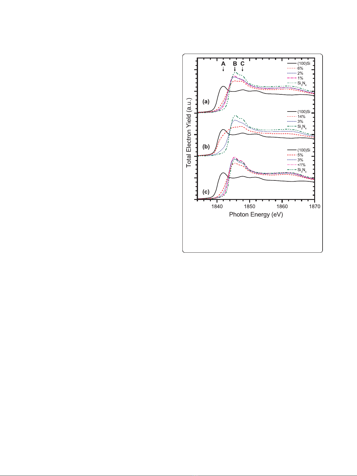
The electronic structure was probed through X-ray
absorption near edge structure experiments at the sili-
con K- and L
3,2
-edges, where differences in structure
within the films can be identified by shifts in their spec-
tral features [25-29]. The XANES measurements per-
formed at the silicon K-edge for AD films from each
system are shown in Figure 3, which reveal common
trends in the Si-nc structure. The spectra of the ICP
CVD films were measured from 2-μm-thick films, much
larger than the information depth at either absorption
edge [30], to ensure that the substrate would not contri-
bute to the TEY or FLY. However, through further
experiments, it has since been found that film thick-
nesses greater than 1500 Å are sufficient not to exhibit
substrate effects in the TEY data at the Si K-edge, or
either the TEY or FLY data at the Si L
3,2
-edge. A low
doped, n-type (100) silicon wafer was used as a crystal-
line silicon reference for all of the XANES experiments,
and the Si
3
N
4
referencesamplewasanADICPCVD
film with stoichiometric composition. As the silicon
content is increased in the films, the absorption edge
shifts to lower energies because of the increase of the
Si-Si resonance peak at 1842 eV and reduction of the
peak related to Si-N bonding located at 1845.5 eV. The
weak Si-O peak at 1848 eV in the crystalline silicon
reference spectrum arises from the native oxide layer
formed at the silicon surface while any Si-O signal
exhibited by the SRSN films originates from oxygen
contamination at the surface of the film and should not
be taken as an indication of Si-O bonding within the
bulk of these films. Figure 4 compares the silicon L
3,2
-
edge spectra for PECVD and ICP CVD AD films. Both
sets of films follow similar trends, with the Si-N reso-
nance peak ranging between 103.8 to 104.5 eV as it
shifts to lower energies and broadens at higher excess
silicon concentrations. However, the PECVD films have
a well-defined Si-Si absorption edge at 99.7 eV, which is
absent in the ICP CVD-deposited films. The prominence
of the absorption edge in PECVD films could be attribu-
ted to a difference in the Si-nc structure or the genera-
tion of a greater number of nucleation sites for Si-nc
formation resulting from the dissociation of hydrogen
from the NH
3
process gas. Unfortunately, the ECR
PECVD films were too thin to avoid a large background
signal from the silicon substrate at these energies, and
so they have not been included in any of the Si L
3,2
-
edge comparisons.
Figures 5 and 6 show the changes in the Si K- and
L
3,2
-edge XANES spectra for two ICP CVD grown films,
Figure 3 TEY-XANES spectra for (a) PECVD, (b) ECR PECVD, and
(c) ICP CVD AD films at the Si K-edge.A,B, and Cindicate the
peak positions for Si-Si, Si-N, and Si-O resonances, respectively. The
percentages in the legend refer to the excess silicon content of the
SRSN films.
Wilson et al.Nanoscale Research Letters 2011, 6:168
http://www.nanoscalereslett.com/content/6/1/168
Page 5 of 12


%20--%3e%3cdefs%3e%3cstyle%3e%20.st0%20{%20fill:%20%23fff;%20}%20.st1%20{%20fill:%20%237800fa;%20}%20%3c/style%3e%3c/defs%3e%3cpath%20class='st1'%20d='M117.78,12.18H43.11c2.9,3.47,4.65,7.94,4.65,12.82,0,5.6-2.3,10.66-6.01,14.29h76.02l7.22-13.56-7.22-13.56Z'/%3e%3cg%3e%3cpath%20class='st0'%20d='M53.58,26.17h-.59v-1.46h.59v-4.96h2.83c1.78,0,2.67.94,2.67,2.82v5.76c0,1.87-.89,2.81-2.67,2.81h-2.83v-4.96ZM55.36,21.37v3.34h1.1v1.46h-1.1v3.34h1.01c.61,0,.91-.37.91-1.1v-5.93c0-.74-.3-1.1-.91-1.1h-1.01Z'/%3e%3cpath%20class='st0'%20d='M65.99,31.14h-1.8l-.31-2.07h-2.19l-.31,2.07h-1.64l1.82-11.39h2.62l1.82,11.39ZM65.28,18.04c-.25.46-.51.77-.75.94-.21.15-.47.22-.79.22-.26,0-.57-.07-.92-.22l-.38-.15c-.14-.05-.26-.07-.37-.07-.3,0-.53.18-.71.54l-.91-.68c.25-.46.51-.77.75-.94.21-.14.48-.21.79-.21.26,0,.57.07.92.21l.38.15c.14.05.26.07.37.07.3,0,.53-.18.71-.54l.91.68ZM61.91,27.52h1.73l-.87-5.76-.87,5.76Z'/%3e%3cpath%20class='st0'%20d='M74.53,26.89v1.52c0,1.91-.89,2.86-2.67,2.86s-2.67-.95-2.67-2.86v-5.93c0-1.91.89-2.86,2.67-2.86s2.67.95,2.67,2.86v1.11h-1.69v-1.22c0-.75-.31-1.12-.93-1.12s-.93.37-.93,1.12v6.15c0,.74.31,1.11.93,1.11s.93-.37.93-1.11v-1.63h1.69Z'/%3e%3cpath%20class='st0'%20d='M81.4,31.14h-1.8l-.31-2.07h-2.19l-.31,2.07h-1.64l1.82-11.39h2.62l1.82,11.39ZM75.9,19.2l1.52-1.91h1.71l1.51,1.91h-1.61l-.76-.95-.75.95h-1.61ZM77.32,27.52h1.73l-.87-5.76-.87,5.76ZM83.1,15.99l-1.76,1.91h-1.26l1.17-1.91h1.86Z'/%3e%3cpath%20class='st0'%20d='M84.86,19.75c1.78,0,2.67.94,2.67,2.82v1.48c0,1.87-.89,2.81-2.67,2.81h-.85v4.28h-1.79v-11.39h2.64ZM84.01,21.37v3.86h.85c.58,0,.87-.36.87-1.08v-1.71c0-.71-.29-1.07-.87-1.07h-.85Z'/%3e%3cpath%20class='st0'%20d='M93.51,19.75c1.78,0,2.67.94,2.67,2.82v1.48c0,1.87-.89,2.81-2.67,2.81h-.85v4.28h-1.79v-11.39h2.64ZM92.66,21.37v3.86h.85c.58,0,.87-.36.87-1.08v-1.71c0-.71-.29-1.07-.87-1.07h-.85Z'/%3e%3cpath%20class='st0'%20d='M98.8,31.14h-1.79v-11.39h1.79v4.88h2.03v-4.88h1.83v11.39h-1.83v-4.88h-2.03v4.88Z'/%3e%3cpath%20class='st0'%20d='M105.36,24.55h2.46v1.62h-2.46v3.34h3.09v1.63h-4.88v-11.39h4.88v1.63h-3.09v3.18ZM108.17,17.29l-1.76,1.91h-1.26l1.17-1.91h1.86Z'/%3e%3cpath%20class='st0'%20d='M112.2,19.75c1.78,0,2.67.94,2.67,2.82v1.48c0,1.87-.89,2.81-2.67,2.81h-.85v4.28h-1.79v-11.39h2.64ZM111.35,21.37v3.86h.85c.58,0,.87-.36.87-1.08v-1.71c0-.71-.29-1.07-.87-1.07h-.85Z'/%3e%3c/g%3e%3ccircle%20class='st1'%20cx='25'%20cy='25'%20r='20'/%3e%3cpath%20class='st0'%20d='M32.78,19.27c2.92,0,4.43,2.55,5.28,5.33l.71,2.17c.14.38-.33.75-.71.75h-5.61c.19-.33.24-.71.09-1.08l-.75-2.45c-.43-1.32-.99-2.64-1.79-3.77.75-.57,1.65-.94,2.78-.94h0ZM25,18.38c3.25,0,4.9,2.78,5.89,5.89l.76,2.45c.14.42-.33.8-.8.8h-11.69c-.42,0-.94-.38-.8-.8l.75-2.45c.99-3.11,2.64-5.89,5.89-5.89h0ZM25,11.35c1.74,0,3.11,1.37,3.11,3.11s-1.37,3.11-3.11,3.11-3.11-1.41-3.11-3.11,1.41-3.11,3.11-3.11h0ZM17.27,19.27c1.08,0,1.98.38,2.73.94-.8,1.13-1.37,2.45-1.74,3.77l-.8,2.45c-.14.38-.05.75.09,1.08h-5.56c-.42,0-.9-.38-.75-.75l.71-2.17c.9-2.78,2.41-5.33,5.33-5.33h0ZM17.27,12.91c1.51,0,2.78,1.27,2.78,2.83s-1.27,2.83-2.78,2.83-2.83-1.27-2.83-2.83,1.27-2.83,2.83-2.83h0ZM32.78,12.91c1.56,0,2.78,1.27,2.78,2.83s-1.23,2.83-2.78,2.83-2.83-1.27-2.83-2.83,1.27-2.83,2.83-2.83h0ZM27.07,28.56v.09c0,.57-.24,1.08-.61,1.46h0v.05c-.38.33-.9.57-1.46.57s-1.08-.24-1.46-.61h0c-.38-.38-.61-.9-.61-1.46v-.09h1.41v.09c0,.19.05.38.19.47v.05c.09.09.28.19.47.19s.38-.09.47-.19v-.05c.14-.09.24-.28.24-.47t-.05-.09h1.41ZM30.99,28.56v.09c0,1.65-.66,3.16-1.74,4.24-1.08,1.08-2.59,1.79-4.24,1.79s-3.16-.71-4.24-1.79l-.05-.05c-1.04-1.08-1.7-2.55-1.7-4.2v-.09h1.41v.09c0,1.27.47,2.4,1.27,3.25h.05c.85.85,1.98,1.37,3.25,1.37s2.4-.52,3.25-1.37c.85-.8,1.37-1.98,1.37-3.25v-.09h1.37ZM34.99,28.56v.09c0,2.78-1.13,5.28-2.92,7.07-1.79,1.79-4.29,2.92-7.07,2.92s-5.23-1.13-7.07-2.92c-1.79-1.79-2.92-4.29-2.92-7.07v-.09h1.41v.09c0,2.4.94,4.53,2.5,6.08,1.56,1.56,3.72,2.5,6.08,2.5s4.52-.94,6.08-2.5c1.56-1.56,2.5-3.68,2.5-6.08v-.09h1.41Z'/%3e%3c/svg%3e)