
NANO EXPRESS Open Access
Effect of the Nd content on the structural and
photoluminescence properties of silicon-rich
silicon dioxide thin films
Olivier Debieu, Julien Cardin, Xavier Portier, Fabrice Gourbilleau
*
Abstract
In this article, the microstructure and photoluminescence (PL) properties of Nd-doped silicon-rich silicon oxide
(SRSO) are reported as a function of the annealing temperature and the Nd concentration. The thin films, which
were grown on Si substrates by reactive magnetron co-sputtering, contain the same Si excess as determined by
Rutherford backscattering spectrometry. Fourier transform infrared (FTIR) spectra show that a phase separation
occurs during the annealing because of the condensation of the Si excess resulting in the formation of silicon
nanoparticles (Si-np) as detected by high-resolution transmission electron microscopy and X-ray diffraction (XRD)
measurements. Under non-resonant excitation at 488 nm, our Nd-doped SRSO films simultaneously exhibited PL
from Si-np and Nd
3+
demonstrating the efficient energy transfer between Si-np and Nd
3+
and the sensitizing effect
of Si-np. Upon increasing the Nd concentration from 0.08 to 4.9 at.%, our samples revealed a progressive
quenching of the Nd
3+
PL which can be correlated with the concomitant increase of disorder within the host
matrix as shown by FTIR experiments. Moreover, the presence of Nd-oxide nanocrystals in the highest Nd-doped
sample was established by XRD. It is, therefore, suggested that the Nd clustering, as well as disorder, are
responsible for the concentration quenching of the PL of Nd
3+
.
Introduction
Over the last decade, there has been an increasing inter-
est toward nanomaterials for novel applications. One of
the challenging fields concerns silicon-compatible light
sources which are getting more and more attractive
since they can be integrated to microelectronics devices
[1]. Amorphous SiO
2
is an inefficient host matrix for
the photoluminescence (PL) of Nd
3+
ions since, on the
one hand, the absorption cross section of Nd is low (1 ×
10
-20
cm
2
) and, on the other hand, the Nd solubility in
silica is limited by clustering [2 ,3], which quenches the
PL of the rare earth (RE) ions [4,5]. However, since the
discovery of the sensitizing effect of silicon nanoparticles
(Si-np)towardtheREions[6],RE-dopeda-SiO
2
films
containing Si-np are promising candidates for the
achievement of future photonic devices. In such nano-
composites, Nd
3+
ions benefit from the high absorption
cross section of Si-np (1-100 × 10
-17
cm
2
) by an efficient
energy transfer mechanism, which enables the PL effi-
ciency of RE ions to be enhanced by 3-4 orders of mag-
nitude offering interesting opportunities for the
achievement of future practical devices optically excited.
In contrast to Er
3+
ions [6-8], such materials doped with
Nd have not been widely investigated and, accordingly,
the energy transfer mechanism between Si-np and Nd
3+
ions, and its limitation [9-16]. Several authors have
demonstrated that the energytransferismoreeffective
with small Si-np [10,11]. Seo et al. [11] have observed a
decrease of the PL intensity of Nd
3+
ions upon increas-
ing the Si excess, i.e., increasing the Si-np average size.
They concluded that only small Si-np which present
excitonic states with a sufficient energy band-gap can
excite the
4
F
3/2
level of Nd
3+
ions. Several groups, which
studied the effect of the Nd concentration in the PL
properties of Nd-doped Si-np/SiO
2
demonstrated
that the PL of Nd
3+
ions is more efficient at low Nd
concentration [12,13].
The object of the present investigation is therefore to
characterize the PL properties of nanostructured thin
films containing a low concentration of Si excess as a
* Correspondence: fabrice.gourbilleau@ensicaen.fr
CIMAP, UMR CNRS/CEA/ENSICAEN/UCBN, Ensicaen 6 Bd Maréchal Juin,
14050 Caen Cedex 4, France
Debieu et al.Nanoscale Research Letters 2011, 6:161
http://www.nanoscalereslett.com/content/6/1/161
© 2011 Debieu et al; licensee Springer. This is an Open Access article distributed under the terms of the Creative Commons Attribution
License (http://creativecommons.org/licenses/by/2.0), which permits unrestricted use, distribution, and reproduction in any medium,
provided the original work is properly cited.
function of the Nd concentration and the annealing
temperature in relation with their microstructures. The
Nd-doped silicon-rich silicon oxide (SRSO) thin layers
were synthesized by reactive magnetron co-sputtering.
Their microstructures were examined using high-
resolution transmission electron microscopy (HRTEM),
X-ray diffraction (XRD), and Fourier transform infrared
(FTIR) spectroscopy. We could notably establish the
proper conditions to obtain efficient PL of Nd
3+
but
also describe its limitations.
Experiment
In this study, Nd-doped SRSO thin layers were depos-
ited at room temperature on p-typeSiwafersbyareac-
tive magnetron RF co-sputtering method that consists in
sputtering simultaneously a pure SiO
2
target topped
with Nd
2
O
3
chips. The Nd content was monitored by
the surface ratio between the Nd
2
O
3
chips and the SiO
2
target. The sputtering gas was a mixture of argon and
hydrogen; the latter enables us to control the Si excess
of the deposited layers by reacting with oxide species in
theplasma[17].Thesamplesweresubsequently
annealed at high temperature ranging from 900 to
1100 °C in a dry nitrogen flow.
The composition of the deposited layers was deter-
mined by Rutherford backscattering spectrometry, while
microstructural analyses were performed using of XRD
and HRTEM on samples prepared in the cross-sectional
configuration using a JEOL 2010F (200 kV). The infra-
red absorption properties were investigated unsing a
Nicolet Nexus FTIR spectrometer at Brewster’s
incidence.
Room temperature PL measurements were performed
using an argon ion laser operating at 488 nm (7.6 W/
cm
2
) as excitation source. This excitation wavelength is
non-resonant with Nd
3+
ions so that only an indirect
excitation of Nd can occur [13,15]. The visible spectra
were recorded using a fast photomultiplier (Hamamatsu)
after dispersion of the PL with a Jobin-Yvon TRIAX 180
monochromator, while the infrared PL was measured
using a Jobin-Yvon THR 1000 monochromator mounted
with a cooled Ge detector and a lock-in amplifier to
record the near-infrared spectra up to 1.5 μm.
Results
In this study, we were interested in four Nd-doped
SRSO thin films containing the same excess of Si
(7 at.%) with various Nd contents ranging from 0.08 to
4.9 at.%.
Microstructure
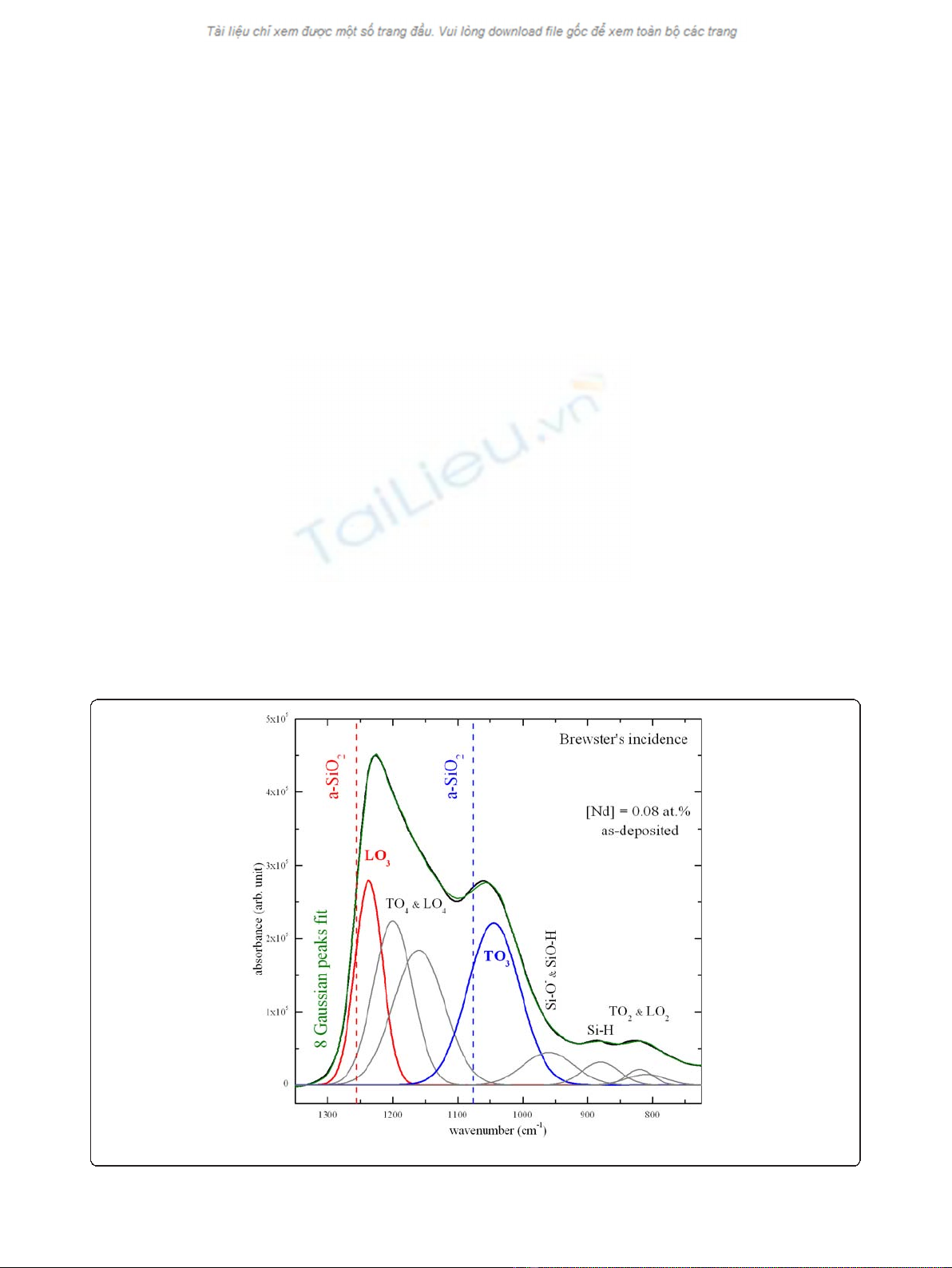
Figure 1 shows the FTIR spectrum of the lowest Nd-
doped sample as-deposited and a fit with eight Gaussian
peaks. Several bands characteristic of amorphous SiO
2
are observed. The two prominent bands at 1236 (red),
and 1052 cm
-1
(blue) are assigned to longitudinal optical
Figure 1 FTIR spectrum of the lowest Nd-doped sample as-deposited.
Debieu et al.Nanoscale Research Letters 2011, 6:161
http://www.nanoscalereslett.com/content/6/1/161
Page 2 of 8
(LO
3
) and transverse optical (TO
3
) phonons of Si-O
bonds, respectively. One can notice that these two
bands are slightly shifted to lower wavenumbers com-
pared to the stoichiometric positions of a-SiO
2
at 1256
and 1076 cm
-1
, respectively. The TO
2
,LO
2
,LO
4
,and
TO
4
vibration modes are also present at 810, 820, 1160,
and 1200 cm
-1
, respectively. In addition to Si-O vibra-
tion modes, a weak absorption band centered at 880
cm
-1
is observed. This peak, which is assigned to Si-H
bonds, disappears after annealing because of the hydro-
gen desorption.
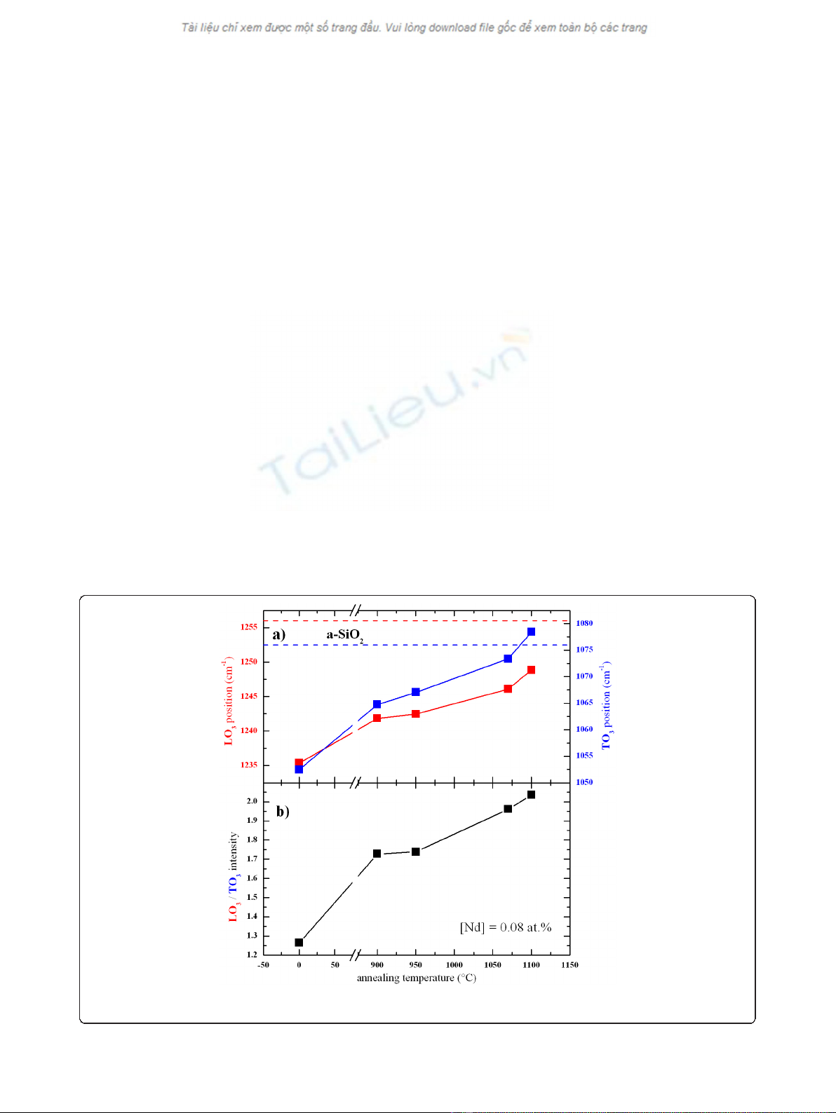
Figure 2a shows the evolution of the positions of the
LO
3
and TO
3
vibration modes, and the LO
3
/TO
3
inten-
sity ratio, as a function of the annealing temperature.
One can observe that, while the annealing temperature
was increased, the TO
3
and LO
3
peaks’positions pro-
gressively shifted to higher wavenumbers toward their
respective stoichiometric positions. It is explained by the
phase separation that results in the formation of Si-np
[18,19]. The increase of the LO
3
band intensity (see Fig-
ure 2b) is related to the increase of the number of Si-O-
Si bonds at the SiO
x
/Si-np interface [19,20], i.e., the
increase of the density of Si-np [21].
Figure 3 presents the evolution of the FTIR spectra of
samples annealed at 1100 °C as a function of the Nd
concentration. One can observe that the LO
3
band
intensity, which is constant at low Nd concentrations of
0.08 and 0.27 at.%, significantly decreased while the Nd
content was increased from 1.68 to 4.9 at.%. This evolu-
tion contrasts with the one of the TO
4
-LO
4
pair modes.
Indeed, the TO
4
-LO
4
intensity remains constant at low
Nd concentrations of 0.08 and 0.27 at.%, and then, it
progressively increases with increasing Nd content. This
demonstrates that the incorporation of Nd in the thin
films generates disorder in the host SiO
2
matrix.
Moreover, one can notice, in the spectrum of the
highest Nd-doped sample, the emergence of two weak
absorption peaks centered at 910 and 950 cm
-1
which
are assigned to asymmetric mode of Si-O-Nd bonds
[22]. These peaks are located above a shoulder which
can originate from Si-O
-
and Si-OH phonons [23,24].
However, one can exclude the existence of the Si-OH
vibration mode after annealing because of the hydrogen
desorption. The emergenceofthesetwoabsorption
peaks suggests that other phonons are also optically
active in this spectral range.
In Figure 4 is depicted the XRD spectra of the lowest
and highest Nd-doped samples. In the former sample,
one broad band corresponding to a-SiO
2
is observed,
while the pattern of the latter sample indicates the pre-
sence of additional phases. In the 27-32° range, it shows
various sharp peaks that are located above a broad band
Figure 2 Evolutions of the positions of the LO
3
and TO
3
peaks, and the LO
3
/TO
3
intensity ratio, as a function of the annealing
temperature.
Debieu et al.Nanoscale Research Letters 2011, 6:161
http://www.nanoscalereslett.com/content/6/1/161
Page 3 of 8
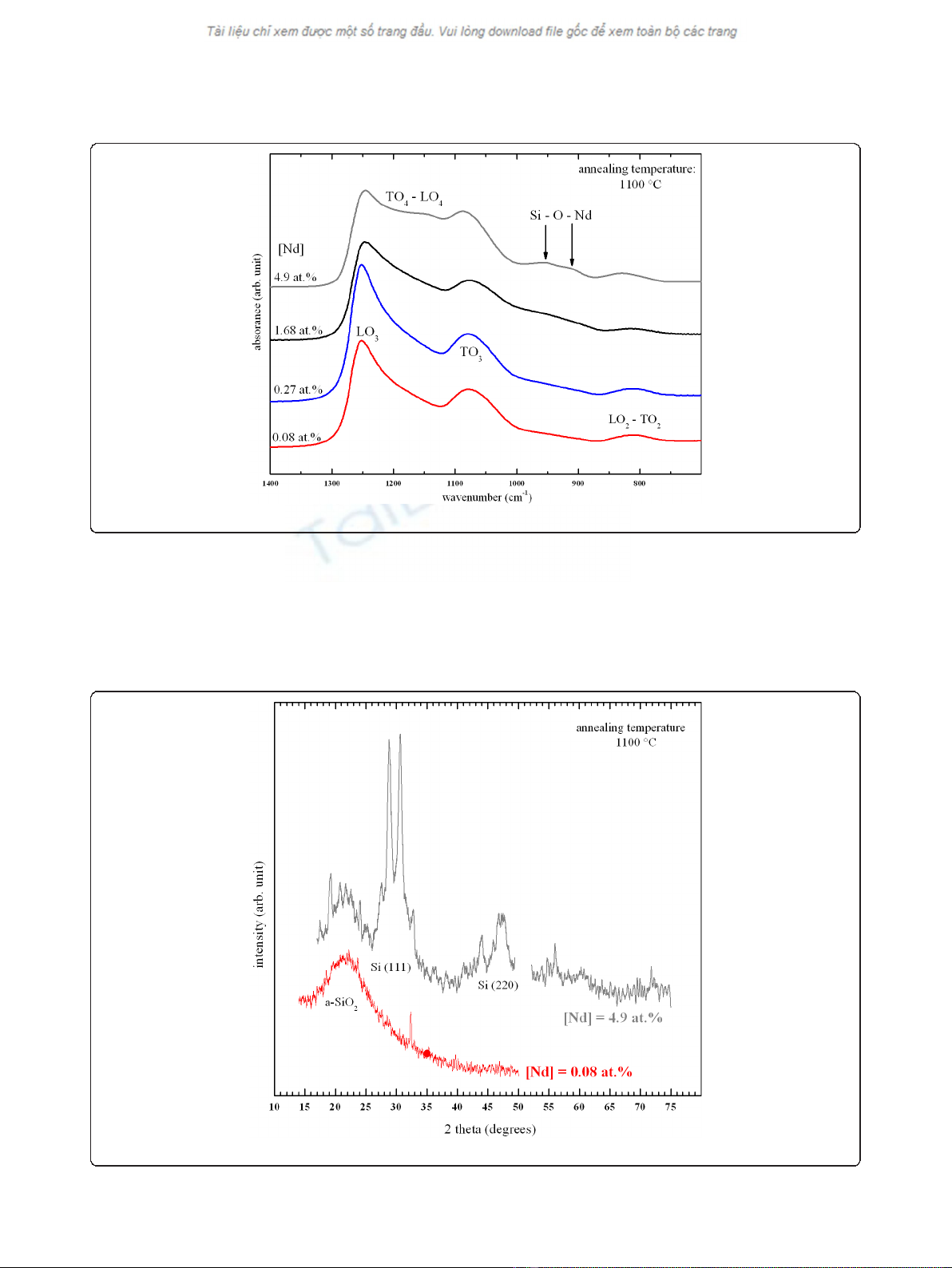
centered at 29°. This peak, and the 48° one, indicate the
presence of nanocrystalline Si [21,25], while the sharp
and intense peaks located at 27.6°, 28.8°, and 30.7° are
assigned to Nd
2
O
3
crystals. However, the 28.8° peak
may result from both crystalline Si and Nd
2
O
3
.Itis
interesting to note that the 27.6° and 30.7° peaks fairly
concur with the ones observed in neodymia-silica com-
posites containing Nd
2
O
3
nanocrystals by several groups
[2,3]. As a consequence, the presence of Nd
2
O
3
and Si
nanocrystals in the highest Nd-doped sample is estab-
lished, while no crystalline phases are detected in the
low Nd-doped one.
Figure 3 Evolution of the FTIR spectra as a function of the Nd concentration.
Figure 4 XRD patterns of the highest and lowest Nd-doped samples annealed at 1100 °C.
Debieu et al.Nanoscale Research Letters 2011, 6:161
http://www.nanoscalereslett.com/content/6/1/161
Page 4 of 8
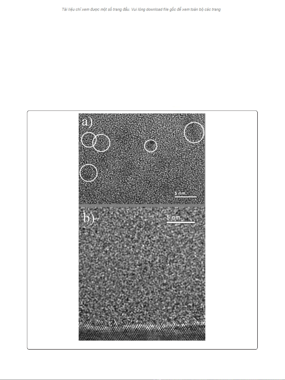
Figure 5 shows the HRTEM images of the two latter
samples investigated by XRD after annealing at 1100 °C.
In the image of the sample with the highest Nd concen-
tration of 4.9 at.% (Figure 5a), one can recognize small
Si nanocrystals because of the lattice fringes correspond-
ing to the Si crystalline feature, while no crystalline
structure was observed in the images of the film con-
taining the lowest Nd concentration of 0.08 at.% (Figure
5b). These two images are in accordance with the XRD
results (see Figure 4). However, one cannot exclude that
the lowest Nd-doped sample could small contain amor-
phous Si-np.
PL spectroscopy
Figure 6 shows the PL spectrum of the lowest Nd-doped
sample after annealing at 1100 °C. In the visible domain,
one can observe a broad PL band that is originating
from quantum-confined excitonic states in small Si-np,
while in the infrared domain, three peaks centered at
around 920, 1100, and 1350 nm are distinguishable and
Figure 5 HRTEM images of the highest (a) and lowest (b) Nd-doped samples annealed at 1100 °C.
Debieu et al.Nanoscale Research Letters 2011, 6:161
http://www.nanoscalereslett.com/content/6/1/161
Page 5 of 8


%20--%3e%3cdefs%3e%3cstyle%3e%20.st0%20{%20fill:%20%23fff;%20}%20.st1%20{%20fill:%20%237800fa;%20}%20%3c/style%3e%3c/defs%3e%3cpath%20class='st1'%20d='M117.78,12.18H43.11c2.9,3.47,4.65,7.94,4.65,12.82,0,5.6-2.3,10.66-6.01,14.29h76.02l7.22-13.56-7.22-13.56Z'/%3e%3cg%3e%3cpath%20class='st0'%20d='M53.58,26.17h-.59v-1.46h.59v-4.96h2.83c1.78,0,2.67.94,2.67,2.82v5.76c0,1.87-.89,2.81-2.67,2.81h-2.83v-4.96ZM55.36,21.37v3.34h1.1v1.46h-1.1v3.34h1.01c.61,0,.91-.37.91-1.1v-5.93c0-.74-.3-1.1-.91-1.1h-1.01Z'/%3e%3cpath%20class='st0'%20d='M65.99,31.14h-1.8l-.31-2.07h-2.19l-.31,2.07h-1.64l1.82-11.39h2.62l1.82,11.39ZM65.28,18.04c-.25.46-.51.77-.75.94-.21.15-.47.22-.79.22-.26,0-.57-.07-.92-.22l-.38-.15c-.14-.05-.26-.07-.37-.07-.3,0-.53.18-.71.54l-.91-.68c.25-.46.51-.77.75-.94.21-.14.48-.21.79-.21.26,0,.57.07.92.21l.38.15c.14.05.26.07.37.07.3,0,.53-.18.71-.54l.91.68ZM61.91,27.52h1.73l-.87-5.76-.87,5.76Z'/%3e%3cpath%20class='st0'%20d='M74.53,26.89v1.52c0,1.91-.89,2.86-2.67,2.86s-2.67-.95-2.67-2.86v-5.93c0-1.91.89-2.86,2.67-2.86s2.67.95,2.67,2.86v1.11h-1.69v-1.22c0-.75-.31-1.12-.93-1.12s-.93.37-.93,1.12v6.15c0,.74.31,1.11.93,1.11s.93-.37.93-1.11v-1.63h1.69Z'/%3e%3cpath%20class='st0'%20d='M81.4,31.14h-1.8l-.31-2.07h-2.19l-.31,2.07h-1.64l1.82-11.39h2.62l1.82,11.39ZM75.9,19.2l1.52-1.91h1.71l1.51,1.91h-1.61l-.76-.95-.75.95h-1.61ZM77.32,27.52h1.73l-.87-5.76-.87,5.76ZM83.1,15.99l-1.76,1.91h-1.26l1.17-1.91h1.86Z'/%3e%3cpath%20class='st0'%20d='M84.86,19.75c1.78,0,2.67.94,2.67,2.82v1.48c0,1.87-.89,2.81-2.67,2.81h-.85v4.28h-1.79v-11.39h2.64ZM84.01,21.37v3.86h.85c.58,0,.87-.36.87-1.08v-1.71c0-.71-.29-1.07-.87-1.07h-.85Z'/%3e%3cpath%20class='st0'%20d='M93.51,19.75c1.78,0,2.67.94,2.67,2.82v1.48c0,1.87-.89,2.81-2.67,2.81h-.85v4.28h-1.79v-11.39h2.64ZM92.66,21.37v3.86h.85c.58,0,.87-.36.87-1.08v-1.71c0-.71-.29-1.07-.87-1.07h-.85Z'/%3e%3cpath%20class='st0'%20d='M98.8,31.14h-1.79v-11.39h1.79v4.88h2.03v-4.88h1.83v11.39h-1.83v-4.88h-2.03v4.88Z'/%3e%3cpath%20class='st0'%20d='M105.36,24.55h2.46v1.62h-2.46v3.34h3.09v1.63h-4.88v-11.39h4.88v1.63h-3.09v3.18ZM108.17,17.29l-1.76,1.91h-1.26l1.17-1.91h1.86Z'/%3e%3cpath%20class='st0'%20d='M112.2,19.75c1.78,0,2.67.94,2.67,2.82v1.48c0,1.87-.89,2.81-2.67,2.81h-.85v4.28h-1.79v-11.39h2.64ZM111.35,21.37v3.86h.85c.58,0,.87-.36.87-1.08v-1.71c0-.71-.29-1.07-.87-1.07h-.85Z'/%3e%3c/g%3e%3ccircle%20class='st1'%20cx='25'%20cy='25'%20r='20'/%3e%3cpath%20class='st0'%20d='M32.78,19.27c2.92,0,4.43,2.55,5.28,5.33l.71,2.17c.14.38-.33.75-.71.75h-5.61c.19-.33.24-.71.09-1.08l-.75-2.45c-.43-1.32-.99-2.64-1.79-3.77.75-.57,1.65-.94,2.78-.94h0ZM25,18.38c3.25,0,4.9,2.78,5.89,5.89l.76,2.45c.14.42-.33.8-.8.8h-11.69c-.42,0-.94-.38-.8-.8l.75-2.45c.99-3.11,2.64-5.89,5.89-5.89h0ZM25,11.35c1.74,0,3.11,1.37,3.11,3.11s-1.37,3.11-3.11,3.11-3.11-1.41-3.11-3.11,1.41-3.11,3.11-3.11h0ZM17.27,19.27c1.08,0,1.98.38,2.73.94-.8,1.13-1.37,2.45-1.74,3.77l-.8,2.45c-.14.38-.05.75.09,1.08h-5.56c-.42,0-.9-.38-.75-.75l.71-2.17c.9-2.78,2.41-5.33,5.33-5.33h0ZM17.27,12.91c1.51,0,2.78,1.27,2.78,2.83s-1.27,2.83-2.78,2.83-2.83-1.27-2.83-2.83,1.27-2.83,2.83-2.83h0ZM32.78,12.91c1.56,0,2.78,1.27,2.78,2.83s-1.23,2.83-2.78,2.83-2.83-1.27-2.83-2.83,1.27-2.83,2.83-2.83h0ZM27.07,28.56v.09c0,.57-.24,1.08-.61,1.46h0v.05c-.38.33-.9.57-1.46.57s-1.08-.24-1.46-.61h0c-.38-.38-.61-.9-.61-1.46v-.09h1.41v.09c0,.19.05.38.19.47v.05c.09.09.28.19.47.19s.38-.09.47-.19v-.05c.14-.09.24-.28.24-.47t-.05-.09h1.41ZM30.99,28.56v.09c0,1.65-.66,3.16-1.74,4.24-1.08,1.08-2.59,1.79-4.24,1.79s-3.16-.71-4.24-1.79l-.05-.05c-1.04-1.08-1.7-2.55-1.7-4.2v-.09h1.41v.09c0,1.27.47,2.4,1.27,3.25h.05c.85.85,1.98,1.37,3.25,1.37s2.4-.52,3.25-1.37c.85-.8,1.37-1.98,1.37-3.25v-.09h1.37ZM34.99,28.56v.09c0,2.78-1.13,5.28-2.92,7.07-1.79,1.79-4.29,2.92-7.07,2.92s-5.23-1.13-7.07-2.92c-1.79-1.79-2.92-4.29-2.92-7.07v-.09h1.41v.09c0,2.4.94,4.53,2.5,6.08,1.56,1.56,3.72,2.5,6.08,2.5s4.52-.94,6.08-2.5c1.56-1.56,2.5-3.68,2.5-6.08v-.09h1.41Z'/%3e%3c/svg%3e)