
JOURNAL OF SCIENCE AND TECHNOLOGY DONG NAI TECHNOLOGY UNIVERSITY
64
Special Issue
STUDY OF THE ROOM-TEMPERATURE LASING OF LEAD
BROMIDE PEROVSKITE THIN FILMS VIA SOLVENT
ENGINEERING
Khai Chu Thanh*
Dong Nai Technology University
*Corresponding author: Chu Thanh Khai, chuthanhkhai@dntu.edu.vn
1. INTRODUCTION Hybrid metal-halide perovskites are
promising materials in optoelectronics; their
long carrier lifetimes, direct bandgaps, and
GENERAL INFORMATION
ABSTRACT
Received date: 23/03/2024
Recent years have seen a significant surge in attention
towards hybrid metal-halide perovskites, primarily for
their remarkable optoelectronic properties: long carrier
lifetimes; direct bandgaps--and large absorption
coefficients. Although we've demonstrated the use of
low-temperature solution-processed perovskites for
lasing, achieving this at room temperature still poses an
ongoing challenge. This study introduces our innovative
approach—a solvent-engineering technique—to
fabricate lead bromide perovskite thin films and create
dense surface morphologies that promote room-
temperature lasing. We achieved the production of
homogeneous perovskite films with enhanced optical
properties by optimizing precursor solutions and
deposition parameters. Photoluminescence
measurements demonstrated efficient room-temperature
lasing above a specific optical pumping density,
characterized by sharp emission peaks and narrow
linewidths. The dense morphology of the perovskite
films found confirmation through scanning electron
microscopy, while multi-peaks in lasing modes indicated
random lasing phenomena presence. The feasibility of
room-temperature lasing in lead bromide perovskite thin
films shines through our findings, underlining the
potential for practical applications as compact and
energy-efficient laser sources.
Revised date: 08/05/2024
Accepted date: 01/08/2024
KEYWORD
Laser luminescence;
Optoelectronic;
Perovskite thin films;
Solvent-engineering technique.

65
JOURNAL OF SCIENCE AND TECHNOLOGY DONG NAI TECHNOLOGY UNIVERSITY
Special Issue
large absorption coefficients present
remarkable properties (Hu et al., 2021). These
unique characteristics render them highly
attractive for a plethora of applications: solar
cells, light-emitting diodes, photodetectors--
even lasers (Yang et al., 2015).
Despite successfully demonstrating lasing
in low-temperature solution-processed
perovskites, achieving room temperature lasing
action--a particularly desirable attribute for
practical applications due to its ease of
integration and operational convenience--
among the diverse applications of perovskite
materials remains a significant challenge. This
paper hones in on achieving room-temperature
lasing in lead bromide perovskite thin films
using a solvent-engineering strategy (Zai et al.,
2018). This versatile technique of controlling
the morphology and crystallinity of such
materials has demonstrated potential for
boosting performance across different
optoelectronic devices. With meticulous
manipulation of precursor solutions and
deposition parameters, dense yet uniform
perovskite films that promote efficient lasing
are within reach (Wang et al., 2016).
This work delves into the solvent-
engineering process: a method used to
manufacture lead bromide perovskite thin films
with an ideal morphology and crystalline
structure for room-temperature lasing. It
scrutinizes three factors – solvent composition,
deposition conditions; and annealing
treatments–that influence the optical properties
and lasing characteristics of these perovskite
films. By conducting comprehensive
experimental analysis--including rigorous
characterization tests—we establish not only
the feasibility but also reliability in achieving
stable room-temperature lasing within lead
bromide perovskite thin film matric(Veldhuis et
al., 2016)s.
Room-temperature lasing, successfully
realized in lead bromide perovskites--this
achievement carries significant implications: it
could foster the development of compact;
efficient, and cost-effective laser sources for a
multitude of optoelectronic applications. Not
only that but also this study's insights enhance
our fundamental understanding of perovskite
optoelectronic properties, thereby paving a
pathway towards future advancements in
devices based on perovskite technology
(Rezaee et al., 2021).
Extensive research efforts in recent years
have been spurred by the quest for efficient and
stable lasing in metal-halide perovskites. This
section offers a concise overview of pivotal
studies on perovskite-based lasing, as well as
the strategies engaged to bolster its
performance. In 2014, breakthrough research
showcased the potential of low-temperature
solution-processed perovskite materials as gain
media for optically pumped lasers; notably, this
marked a significant milestone in lasing action.
Despite these early studies' success—
demonstrating reliable and stable room
temperature lasing remained a formidable
challenge. This unmet hurdle thus incited
deeper scrutiny into novel fabrication
techniques and material optimization strategies:
an exploration that continues to date (Hu et al.,
2021).
Approaches in Solvent Engineering:
Researchers harness the power of solvent
engineering as a potent strategy to customize
the morphology and crystalline characteristics
of perovskite thin films - an approach that
bolsters their optoelectronic performance. With
the meticulous selection of solvent
compositions, control over deposition
parameters, and optimization for annealing
processes; they have indeed accomplished
remarkable feats such as improving film quality,

JOURNAL OF SCIENCE AND TECHNOLOGY DONG NAI TECHNOLOGY UNIVERSITY
66
Special Issue
decreasing defect density – and even
sharpening optical properties. Successful
application extends beyond mere theory into
practice: various perovskite-based devices –
solar cells, light-emitting diodes; and
photodetectors all benefit from these refined
techniques. However, their application in
achieving room-temperature lasing has
received limited attention until recently (Han et
al., 2024).
The researchers have made significant
progress towards achieving room-temperature
lasing in metal-halide perovskite materials.
They've explored innovative approaches such
as interface engineering, surface passivation,
and doping strategies--all aimed at enhancing
the optical gain and stability of perovskite thin
films. Moreover, they've proposed novel device
architectures and cavity designs to achieve
efficient light confinement coupled with
feedback; this is critical for realizing lasing
action under ambient conditions. These
advancements underscore the growing interest
and the potential of perovskite-based lasers for
practical applications (Veldhuis et al., 2016).
Considerable strides have indeed been
made towards achieving room-temperature
lasing in perovskite thin films; however, several
pressing issues still warrant attention – notably
material stability, device reproducibility, and
long-term performance degradation. These
factors continue to impose significant obstacles
to successful commercialization. Therefore – to
fill critical gaps in our understanding of this
complex phenomenon while also addressing
practical concerns regarding large-scale
manufacturing–future research efforts must
focus on two key areas: elucidating the
fundamental mechanisms that govern lasing
behavior within perovskite materials and
developing robust fabrication techniques
capable of scalable production. To unlock the
full potential of perovskite-based lasers in a
broad spectrum of optoelectronic applications,
we must address these challenges: indeed, it is
crucial.
2. EXPERIMENTAL
2.1. Materials and Chemicals
[Supplier Name] provided us with Lead
bromide (PbBr2) and methylammonium
bromide (MABr). We utilized γ-butyrolactone
(GBL) and dimethyl sulfoxide (DMSO), as
organic solvents for the solvent-engineering
process; toluene served as a non-solvent
additive. All chemicals were used as received
without further purification.
2.2. Fabrication of Lead Bromide Perovskite
Thin Films
A consecutive solvent-engineering process
prepared the lead bromide perovskite thin films.
Figure 1(a) describes the solvent engineering
that is adopted in this work. The steps involved
in the fabrication process are as follows:
a. precursor solution preparation: At a ratio
of 7:3 (v/v), an Optimized mixture of GBL and
DMSO solvents was prepared. The powders
PbBr2 and MABr underwent vigorous stirring
in the solvent mix until complete dissolution
occurred.
b. During the spin-coating process, we
applied the as-prepared precursor solution to
UV-O3-cleaned glass substrates at a controlled
spin speed for 30 seconds. As part of this
procedure, we sequentially dripped toluene
onto the spinning substrate; its purpose was not
only retarding the reaction but also aiding in
perovskite crystalline structure formation.
c. Annealing: The researcher annealed the
resultant films at a temperature of 100°C for 30
minutes; this process served to eliminate any
lingering solvents and facilitate the
transformation of intermediate solvate phases
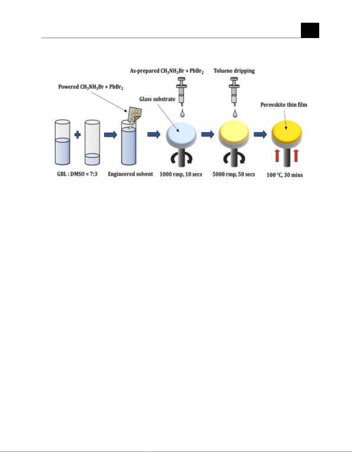
67
JOURNAL OF SCIENCE AND TECHNOLOGY DONG NAI TECHNOLOGY UNIVERSITY
Special Issue
into perovskite crystalline structures. Notably,
the annealing procedure took place within a
glove box filled with nitrogen--an action taken
specifically to thwart oxidation and moisture
contamination.
Figure 1(a). The process of solvent engineering
2.3. Characterization Techniques
The scanning electron microscope (SEM):
characterized the morphology of our prepared
perovskite thin films; we acquired SEM images
to scrutinize their surface morphology, grain
size, and uniformity.
Photoluminescence (PL) Spectroscopy:
Conducting photoluminescence measurements-
-this is an investigation into the optical
properties of perovskite thin films. Under room
temperature conditions, we recorded PL spectra
using a specific instrument; [instrument details]
were utilized for this purpose.
Lasing Characterization
a. An optical pumping setup evaluated the
lasing characteristics of solvent-engineered
lead bromide perovskite thin films: specifically,
they were excited by a [details of laser source]
at room temperature; this investigation utilized
an optical pumping system.
b. Power-Dependent PL Emission: We
acquired power-dependent PL emission spectra
to investigate the emission characteristics of
perovskite thin films under varying optical
pumping densities.
C: Analysis of the Lasing Threshold; By
scrutinizing the onset of sharp emission peaks
in PL spectra--as a function of optical pumping
density, we determined the lasing threshold for
perovskite thin films.
3. RESULTS AND DISCUSSION
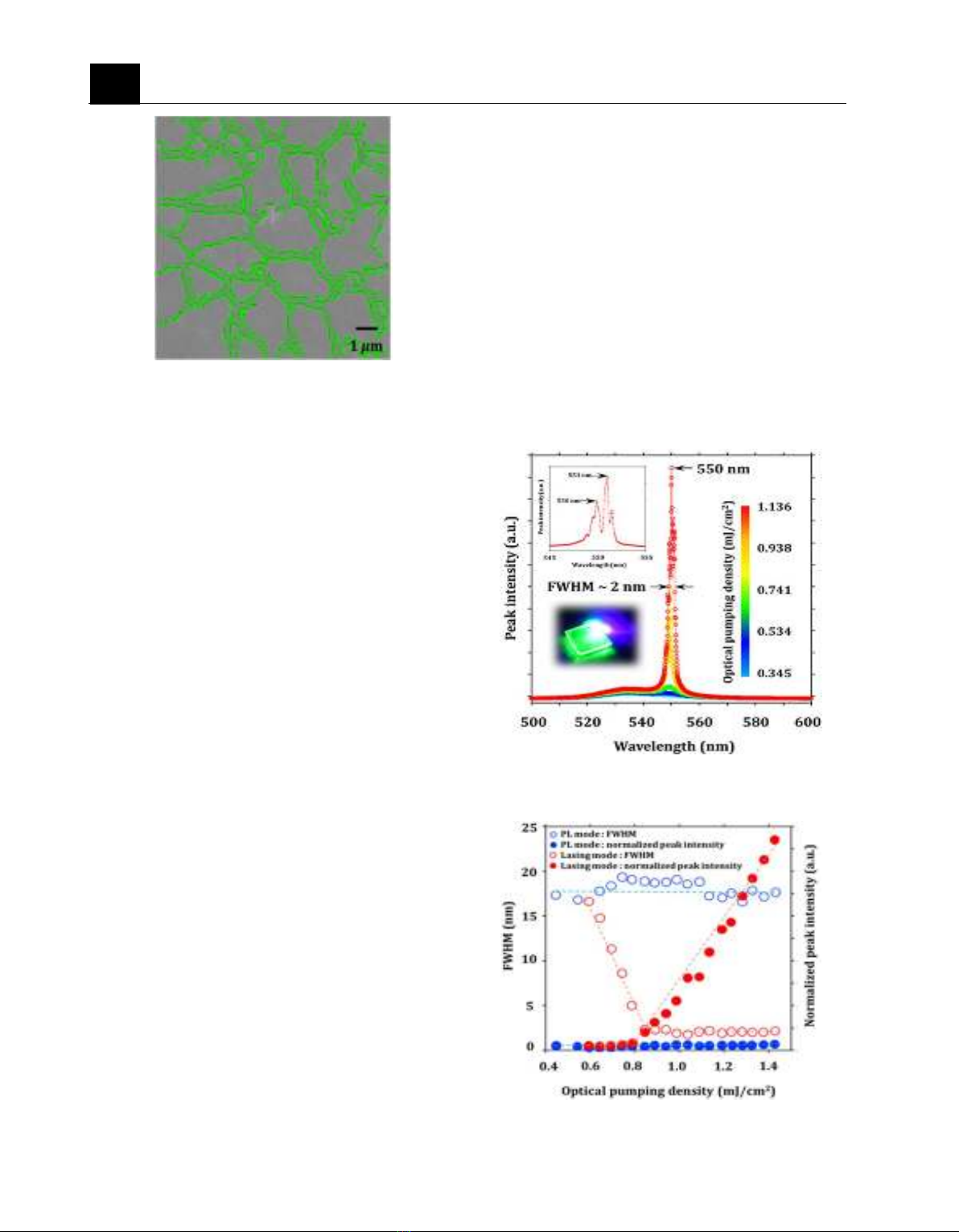
3.1. Morphological Characterization
Fig. 1 reveals dense, uniform surface
morphology without voids on the solvent-
engineered lead bromide perovskite thin films
in Scanning Electron Microscopy (SEM)
images; an analysis of surface area confirms a
homogeneous distribution of perovskite
crystalline grains with an average radius
measuring approximately 1.18 µm--it further
establishes this fact by indicating a filling area
fraction around 89.31%.
JOURNAL OF SCIENCE AND TECHNOLOGY DONG NAI TECHNOLOGY UNIVERSITY
68
Special Issue
Figure 1(b). Scanning electron microscope (SEM)
The process of solvent engineering and a
scanning electron microscope (SEM) image
presenting lead bromide perovskite thin films are
illustrated in Figure 1. In particular, panel (a)
illustrates the preparation method for these films
through consecutive spin-coating procedures
using advanced solvent techniques. Panel (b), on
the other hand, exhibits an SEM image
showcasing dense surface morphology without
any voids in the resultant lead bromide perovskite
thin film. Analysis of surface area reveals a
perovskite crystalline grain filling area fraction of
approximately 89.31%, which denotes a
homogeneous surface morphology. Furthermore,
the average radius for these perovskite crystalline
grains is measured at 1.18 μm.
3.2. Optical Properties and Lasing
Characteristics
We acquired power-dependent
photoluminescence (PL) emission spectra to
explore the optical properties and lasing
behavior of perovskite thin films. Figure 2(a)
demonstrates an increase in emission intensity
as we escalate the optical pumping density.
When operating under the lasing threshold, we
observed broad spontaneous emission modes
with a full width at half maximum (FWHM) of
roughly 18 nm and a center wavelength around
538 nm; this occurred at approximately 0.8
mJ/cm^2 — below that point is where these
phenomena manifested themselves most
prominently.
The perovskite thin films exhibited a sharp
emission peak at approximately 550 nm,
indicating lasing action once they surpassed the
threshold. The Full Width Half Maximum
(FWHM) of the lasing modes also significantly
narrowed to about 2 nm, thereby demonstrating
coherence in their emitted light. This sudden
alteration in emission characteristics is depicted
by the light-light curve at its lasing threshold
(Fig.). 2(b)), provided clear evidence of the
onset of lasing in the perovskite films.
Figure 2(a). The increase in emission intensity as
we increase the optical pump density
Figure 2(b). The light-light curve at its lasing
threshold


![Bài giảng Vật lý đại cương Chương 4 Học viện Kỹ thuật mật mã [Chuẩn SEO]](https://cdn.tailieu.vn/images/document/thumbnail/2025/20250925/kimphuong1001/135x160/46461758790667.jpg)