VNU Journal of Science: Mathematics – Physics, Vol. 41, No. 1 (2025) 61-68
61
Original Article
Effect of Sr Content on Microstructure and Electrical
Properties of Lead-free Ba1-xSrxTiO3 thin Films
Vu Thu Hien1,*, Nguyen Thi Minh Phuong1,2, Vu Ngoc Hung1
1Falculty of Electronic Materials and Devices, Hanoi University of Science and Technology,
1 Dai Co Viet, Hai Ba Trung, Hanoi, Vietnam
2University of Transport Technology, 54 Trieu Khuc, Thanh Xuan, Hanoi, Vietnam
Received 22nd October 2024
Revised 29th November 2024; Accepted 10th March 2025
Abstract: Lead-free barium titanate based Ba1-xSrxTiO3 thin films (x = 0 ÷ 0.45) have been deposited
onto Pt/Ti/SiO2/Si(100) substrate via sol–gel technique. The films were crystallized at temperature
of 650 °C for 30 min in the air. The experimental data displayed that microstructure, dielectric and
ferroelectric properties of the films were strongly influenced by the Sr concentration. All the films
are well formed in a polycrystalline perovskite phase with a shift of diffraction planes toward larger
2θ as increasing Sr content. High resolution scanning electron microscopy images as well as cross-
section profile indicate a dense structure, clear grains and a sharp interface between the film and Pt
electrode. However, the shape and grain size change among Sr-doped films. Series data on
capacitance ˗ voltage measurements reveal that dielectric constant (ε) increases with Sr-dopant
concentration while loss tangent (tanδ) decreases. The optimal dielectric properties are found for
Ba0.55Sr0.45TiO3 (x= 0.45), while Ba0.65Sr0.35TiO3 (x= 0.35) thin films perform better polarization
properties with the maximum polarization of 8.07 C/cm2 under applied electric field of 1,000 kV/cm.
Keywords: Lead-free BST-BZT thin film, chemical solution deposition, microstructure, dielectrics
1. Introduction*
During the past decades, traditional lead zirconate-titanate Pb(Zr,Ti)O3 (PZT) is a common
piezoelectric material that has been used for preparation of electromechanical devices [1]. However,
the high toxicity of lead to the health and environment resulting to the lead-based piezoelectrics are
being replaced with lead-free alternatives [2]. Therefore, lead-free ferroelectrics, currently, withdraw a
lot of research attention. Among the ferroelectric materials, barium titanate based Ba1-xSrxTiO3 (BST)
________
* Corresponding author.
E-mail address: hienvt@itims.edu.vn
https//doi.org/10.25073/2588-1124/vnumap.4974

V. T. Hien et al. / VNU Journal of Science: Mathematics – Physics, Vol. 41, No. 1 (2025) 61-68
62
with distinct perovskite crystalline structure ABO3 is a promising candidate for microelectronic devices
such as nonvolatile random access memory, motion and thermal sensors, phase shifter, tunable microwave and
energy storage devices due to its high dielectric constant and relatively low dielectric loss in a wide frequency
range [3-5]. Essentially, BST is a solid solution of ferroelectric BaTiO3 and paraelectric SrTiO3. According to the
results reported in [6, 7], the polarization and dielectric properties of these materials are dependent on both the off-
center displacement of Ti atom from the elementary-cell octahedron [BO6] and the type of cation A. On the other
hand, to develop these materials for practical application, the preparation of high-quality BST as well as improving
its electrical properties are very important. It has been known from the review articles over the past few years that
Curie temperature (TC) and dielectric properties of BST can be tailored by inserting Sr element into Ba site and
changing Ba/Sr atom ratio. Ba1-xSrxTiO3 is attributed to be ferroelectric and paraelectric when x is in range of 0
÷ 0.3 and 0.4 ÷ 1, respectively [8, 9]. Values of dielectric constant and dielectric loss with composition reported
by various research groups present a wide variation. In general, the optimal permittivity is found for BST thin
films with the composition x ranging from 0.4 to 0.5 [10-12]. Moreover, variations in dielectric constant and
dielectric loss are reported differently for different thin film composition as well as different thickness and
deposition conditions. Therefore, to study the influence of composition, thin films with different composition need
to be fabricated under similar technological conditions.
In the present work, BST (x= 0 ÷ 0.45) thin films were deposited from modified precursor solutions
by the costly effective sol–gel process onto Pt/Ti/SiO2/Si(100) substrates. The effect of Sr/Ba
composition in a precursor solution on the phase structure, the surface morphology, and the electrical
properties of the resultant BST thin films was investigated and discussed.
2. Experimental Details
Raw initiative materials utilized in this work include barium acetate [ (CH3COO)2Ba, ACS reagent
99%, Sigma-Aldrich], strontium acetate [(CH3COO)2Sr, purity 98%, Sigma-Aldrich], titanium(IV)-
isopropoxide [C12H28O4Ti, 98%, Merck] and zirconium(IV)-propoxide [(C12H28O4)Zr, 70% in 1-
propanol, Acros]. Glacial acetic acid (CH3COOH), 2-methoxy ethanol (2-MOE), and acetylacetone
(C5H8O2) were used as the solvent, and chelating agent, respectively. The desired moll ratio of Ba/Sir
according to Ba1-xSrxTiO3 (x=0, 0.25, 0.35, and 0.45 denoted as BT, B75, B65 and B55, respectively)
were weighted and dissolved completely in acetic acid with constant stirring at 120 oC for 5 hours to
form salt precursor. Then, titanium(IV)-isopropoxide and 2-MOE were added into the solution while
keeping continuous stirring at 80 oC for at least 3 hours to obtain BT, B75, B65 and B55 precursors,
respectively. In those solutions acetylacetone was added to stabilize the solution. Various precursors of
BT, B75, B65 and B55 with a fixed concentration of 0.40 M were prepared for depositing thin film.
All thin films were spin-coated onto Pt/Ti/SiO2/Si(100) substrates with the rate of 3,000 rpm for
30 s. The as-coated films were dried at 150 oC for 5 min, then at 450 oC for 10 min using a tube furnace
(TF55030C, Linberg/Blue M). Heating speed selected for the whole temperature processing was 10 oC
per min. These steps were repeated five to ten times to achieve a desired film thickness. Finally, the
films were annealed at 650 oC for 30 min in air to form perovskite phase.
The crystalline phase and crystallographic orientation of the film were examined by using XRD
method (XRD; Bruker, Germany). The surface morphology and thickness of the films were evaluated by
Field emission scanning electron microscopy (FE-SEM, HELIOS 650, USA). For electrical
measurements, ~ 100 nm-thick Pt top-electrodes were sputtered on the surface of the films via a Cr-
mask and lift-off lithography process to form metal–insulator–metal (MIM) capacitors. Squared-pad
sizes of 30×30, 100×100, 150×150, and 200×200 m2 were produced. Capacitance measurement and
hysteresis loop were examined by TF Analyzer 2000 (aix ACCT, Germany). All the measurements were
carried-out at room temperature.
V. T. Hien et al. / VNU Journal of Science: Mathematics – Physics, Vol. 41, No. 1 (2025) 61-68
63
3. Results and Discussion
3.1. Microstructural Properties
From XRD it is seen that the as-deposited films were amorphous, wheeas in the films either
crystallized at temperatures larger 700 °C or spin-coated over 12 coating layers severely appeared
cracks. Therefore, the samples were prepared only with 10 coating layers and thenannealed at 650 °C.
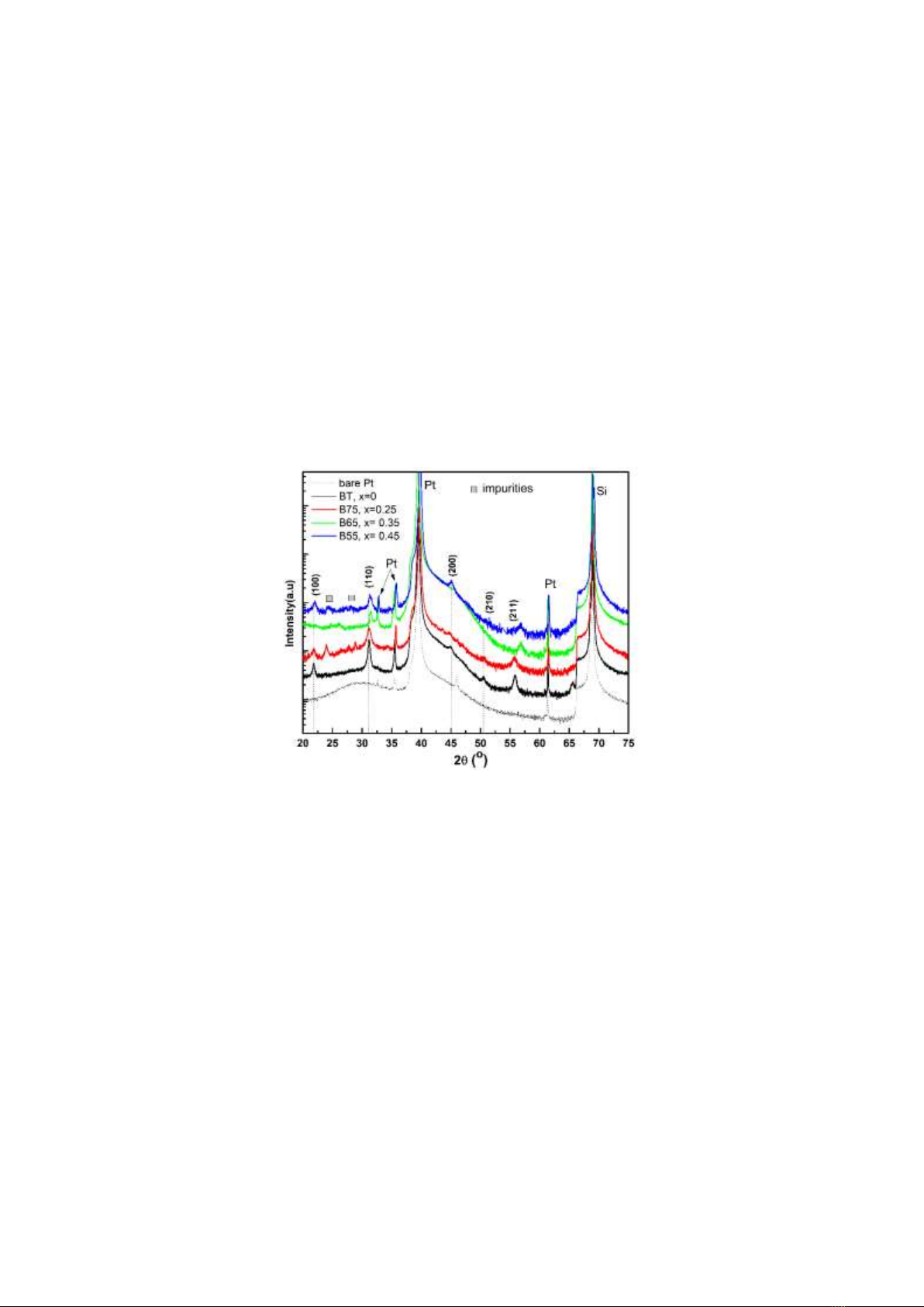
Four XRD patterns of BT, and BT-based thin films with different Sr content in a range of 2 from
20o to 75o are presented in Fig. 1. It can be seen that all the films exhibited well crystallinity. Besides the
peaks of Pt bottom electrode and Si substrate, all XRD patterns have basically well-defined diffraction
planes, including (100), (110), (200), (210) and (211) which relate to tetragonal perovskite structures
[13, 14]. The most intense reflections are of (110) and (210) peaks. B75 and B55 films show peaks
around 24o and 28.8o among the perovskite peaks. The small amount of the second phase is attributed
to be BaCO3 or (Ba,Sr)2TiO4 phases [15, 16].
Figure 1: X-Ray diffraction pattern of barium titanate thin films with various Sr content annealed
at 650 oC/30 min in the air. The Miller indices of the main phase peaks and the peak positions of Pt electrode
and Si substrate as reference are indicated.
It is note that the diffraction peaks shift toward larger diffraction angles as the Sr content increases
from 0 to 0.45, which implies the change in the lattice constant due to the partial substitution of Sr2+ into
BaTiO3 lattice. In comparison to pure BT, the parameters of the unit cell of B75, B65 and B55 may be
reduced because the radius ion of Sr2+ (0.113 nm) is smaller than that of Ba2+ (0.135 nm) [17-19].
The 2 peak shift is most obviously observed at (100), (110) and (211) planes. Fig. 2 displays two
representative XRD patterns of the (110) and (211) peaks as a function of Sr content. These diffraction
peaks are achieved in the range of 2 from 30° to 32° and from 54° to 58°determined by analyzing the
individual peak using Gauss curve fit function. As observed from the shape of the XRD patterns, the
fitting procedure yields a significant decrease of the tetragonal phase content with increase in Sr amount
(Table 1). The results showed that not only the unit cell change but the crystalline grain size also seems
to be decreased since the full width at half maximum (FWHM) of B75, B65 and B55 increases.

V. T. Hien et al. / VNU Journal of Science: Mathematics – Physics, Vol. 41, No. 1 (2025) 61-68
64
Figure 2: XRD profile around 30o to 32o (left) and 54o to 58o (right).
Table 1. 2 and FWHM estimated from (100), (110) and (211) diffraction peaks of BT, B75, B65
and B55 thin films
Planes
(hkl)
Samples
(100)
(110)
(211)
2
(degree)
FWHM
2
(degree)
FWHM
2
(degree)
FWHM
BT, x=0
21.83
0.389
31.18
0.408
55.82
0.673
B75, x=0.25
21.82
0.408
31.18
0.672
55.66
1.266
B65, x= 0.35
--
--
31.48
0.477
56.80
0.600
B55, x= 0.45
22.00
0.513
31.38
0.620
56.72
0.633
Figure 3: SEM images of the top surface of spin-coated BT, B75, B65 and B55 thin films
on Pt electrode. Insert image show cross-section of BT film. The thickness of 10L BT film is 402 nm,
which turns to around 40 nm per a coating layer.
Fig. 3 shows typical SEM images of the surface and cross-sectional morphologies of BT, B75, B65
and B55 thin films. These films are rather dense, smooth and there are no crack. However, the of Ba/Sr
ratio significantly affects to the grain shape and size. BT films show granular shape with the size of 35

V. T. Hien et al. / VNU Journal of Science: Mathematics – Physics, Vol. 41, No. 1 (2025) 61-68
65
- 100 nm. Meanwhile, the Sr-doped films give particles of round shape and rather small size. Similar
behavior has been reported for CSD and PLD derived BST and BSZT thin films with a smaller grain
sizes [17, 20]. Slight deviation in the grain size with increase of Sr/Ba content is explained due to non-
uniform agglomerates during the process. During annealing, the nucleation as well as the grain growth
process for the different composition in the perovskite materials occurred differently [7]. The grain size of
the film shows a little change with the increase of the Sr concentration. Grains with slightly increased size
and improved crystalline structure are observed clearer for the sample B55, then B65, and B75.
Surface mapping for BT is confirmed by cross-sectional analysis shown in the insert image in
Fig. 3. One can see that the out-of-plane grain sizes and morphologies are similar to the top surface: the
grains are granular and dense. The total thickness of the BT film is ca. 402 nm for 10 coating layers,
which turns out ~ 40 nm per coating layer.
3.2. Dielectric and Ferroelectric Properties
Figure 4: Dielectric constant and loss tangent of BT, B75, B65 and B55 thin films measured at different applied
voltage ranges: (a) 5V; (b) 10V; (c) 20V and (d) 30V.
Sr/Ba ratio dependence of the dielectric constant and dielectric loss as function of applied electric
field is given in Fig. 4. Typical butterfly shape of the -E curves is observed at almost applied electric
field range for all thin films, which indicates the presence of ferroelectric phase as expected from XRD
measurements. Furthermore, with the increasing in the electric field, the relative permittivity decreases
and dielectric loss slightly increases. The Ba0.55Sr0.45TiO3 (B55) thin film always possesses the largest
dielectric constant and the decreases with decreasing Sr content down to x = 0. The dielectric constant
at 100 kHz and zero bias for different applied voltage ranges and different Sr compositions are listed in
the Table 2. B55 thin films also exhibit the lowest tan (~ 0.026) and B75 hold the largest one (~ 0.062).


![Bài giảng Vật lý đại cương Chương 4 Học viện Kỹ thuật mật mã [Chuẩn SEO]](https://cdn.tailieu.vn/images/document/thumbnail/2025/20250925/kimphuong1001/135x160/46461758790667.jpg)