VNU Journal of Science: Comp. Science & Com. Eng., Vol. 31, No. 3 (2015) 1-21
An Efficient Implementation of Advanced Encryption
Standard on the Coarse-grained Reconfigurable Architecture
Hung K. Nguyen, Xuan-Tu Tran
SIS Laboratory, VNU University of Engineering and Technology
144 Xuan Thuy road, Cau Giay district, Hanoi, Vietnam
Abstract
The Advanced Encryption Standard (AES) is currently considered as one of the best symmetric-key block
ciphers. The hardware implementation of the AES for hand-held mobile devices or wireless sensor network
nodes is always required to meet the strict constraints in terms of performance, power and cost. Coarse-grained
reconfigurable architectures are recently proposed as the solution that provides high flexibility, high performance
and low power consumption for the next-generation embedded systems. This paper presents a flexible, high-
performance implementation of the AES algorithm on a coarse-grained reconfigurable architecture, called
MUSRA (Multimedia Specific Reconfigurable Architecture). First, we propose a hardware-software partitioning
method for mapping the AES algorithm onto the MUSRA. Second, the parallel and pipelining techniques are
considered thoughtfully to increase total computing throughput by efficiently utilizing the computing resources
of the MUSRA. Some optimizations at both loop transformation level and scheduling level are performed in
order to make better use of instruction-, loop- and task- level parallelism. The proposed implementation has been
evaluated by the cycle-accurate simulator of the MUSRA. Experimental results show that the MUSRA can be
reconfigured to support both encryption and decryption with all key lengths specified in the AES standard. The
performance of the AES algorithm on the MUSRA is better than that of the ADRES reconfigurable processor,
Xilinx Virtex-II, and the TI C64+ DSP.
© 2015 Published by VNU Journal of Science.
Manuscript communication: received 15 December 2013, revised 06 December 2014, accepted 19 January 2015
Corresponding author: Hung K. Nguyen, kiemhung@vnu.edu.vn
Keywords: Coarse-grained Reconfigurable Architecture (CGRA), Advanced Encryption Standard (AES),
reconfigurable computing, parallel processing.
1. Introduction
The fast development of the communication
technology enables the information to be easily
shared globally via the internet, especially with
the Internet of Things (IoT). However, it also
raises the requirement about the secure of the
information, especially the sensitive data such
as password, bank account, personal
information, etc. One method to protect the
sensitive data is using symmetric-key block
cipher before and after sending it over the
network. The Advanced Encryption Standard
(AES), which has been standardized by the
National Institute of Standard and Technology
(NIST) [1], is currently considered as one of the
best symmetric-key block ciphers. With the
block size of 128 bits and the variable key
length of 128 bits, 192 bits or 256 bits, the AES
has been proved to be a robust cryptographic
algorithm against illegal access.
H.K. NGUYEN et al. / VNU Journal of Science: Comp. Science & Com. Eng., Vol. 31, No. 1 (2015) 1-21
2
The hardware implementation of the AES
for modern embedded systems such as hand-
held mobile devices or wireless sensor network
(WSN) nodes always gives designers some
challenges such as reducing chip area and
power consumption, increasing application
performance, shortening time-to-market, and
simplifying the updating process. Besides, these
systems are often designed not only for a
specific application but also for multiple
applications. Such sharing of resources by
several applications makes the system cheaper
and more versatile. Application Specific
Integrated Circuits (ASICs), Digital Signal
Processors (DSPs), and Application-Specific
Instruction Set Processors (ASIPs), have been
used for implementing the mobile multimedia
systems. However, none of them meets all of
the above challenges [2]. The software
implementation of the AES algorithm by using
processors (e.g. [3]) are usually very flexible
and usually targets at the applications at where
flexibility has a higher priority than the
implementation efficiency in terms of power
consumption, area, and performance. In contrast,
the ASIC implementation of the AES algorithm
(e.g. [4]) usually offers the optimized
performance and power consumption. However,
the drawback of ASIC is lower flexibility.
Moreover, the high price for designing and
manufacturing the chip masks is becoming
increasingly an important factor that limits the
application scope of ASIC. Recently, a very
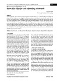
promising solution is the reconfigurable
computing systems (e.g. Zynq-7000 [5],
ADRES [6], etc.) that are integrated many
heterogeneous processing resources such as
software programmable microprocessors (P),
hardwired IP (Intellectual Property) cores,
reconfigurable hardware architectures, etc. as
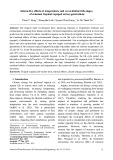
shown in Figure 1. To program such a system, a
target application is first represented
intermediately as a series of tasks that depends
on each other by a Control and Data Flow
Graph (CDFG) [7], and then partitioned and
mapped onto the heterogeneous computational
and routing resources of the system. Especially,
computation-intensive kernel functions of the
application are mapped onto the reconfigurable
hardware so that they can achieve high
performance approximately equivalent to that
of ASIC while maintaining a degree of
flexibility close to that of DSP processors. By
dynamically reconfiguring hardware,
reconfigurable computing systems allow many
hardware tasks to be mapped onto the same
hardware platform, thus reducing the area and
power consumption of the design [8].
CGRA
AHB/CGRA Interface
DPLL
AMBA AHB
PInstruction
Memory
Data Memory
IP cores
Figure 1. System-level application model of CGRA.
The reconfigurable hardware is generally
classified into the Field Programmable Gate
Array (FPGA) and coarse-grained dynamically
reconfigurable architecture (CGRA). A typical
example of the FPGA-based reconfigurable
SoC is Xilinx Zynq-7000 devices [5]. Generally,
FPGAs support the fine-grained reconfigurable
fabric that can operate and be configured at bit-
level. FPGAs are extremely flexible due to their
higher reconfigurable capability. However, the
FPGAs consume more power and have more
delay and area overhead due to greater quantity
of routing required per configuration [9]. This
limits the capability to apply FPGA to mobile
devices. To overcome the limitation of the
FPGA-like fine-grained reconfigurable devices,
H.K. NGUYEN et al. / VNU Journal of Science: Comp. Science & Com. Eng., Vol. 31, No. 1 (2015) 1-21
3
we developed and modeled a coarse-grained
dynamically reconfigurable architecture, called
MUSRA (Multimedia Specific Reconfigurable
Architecture) [10]. The MUSRA is a high-
performance, flexible platform for a domain of
applications in multimedia processing. In
contrast with FPGAs, the MUSRA aims at
reconfiguring and manipulating on the data at
word-level. The MUSRA is proposed to exploit
high data-level parallelism (DLP), instruction-
level parallelism (ILP) and TLP (Task Level
Parallelism) of the computation-intensive loops
of an application. The MUSRA also supports
the capability of dynamic reconfiguration by
enabling the hardware fabrics to be
reconfigured into different functions even if the
system is working.
In this paper, we proposed a solution for
implementing the AES algorithm on the
platform of the MUSRA-based system. The
AES algorithm is firstly analyzed and
optimized, and then HW/SW
(Hardware/Software) partitioned and scheduled
to be executed on the MUSRA-based system.
The experimental results show that our proposal
achieves the throughput of 29.71 instructions
per cycle in average. Our implementation has
been compared to the similar works on ADRES
reconfigurable processor [6], Xilinx Virtex-II
[11], and TI C64+ DSP [3]. Our
implementation is about 6.9 times, 2.2 times,
and 1.6 times better than that of TI C64+ DSP,
Xilinx Virtex-II, and ADRES, respectively.
The rest of the paper is organized as follows.
The MUSRA architecture and the AES
algorithm are presented in Section 2 and
Section 3, respectively. Section 4 presents the
mapping the AES algorithm onto the MUSRA-
based system. In Section 5, simulation results
and the evaluation of the AES algorithm on the
MUSRA-based system in terms of flexibility
and performance are reported and discussed.
Finally, conclusions are given in Section 6.
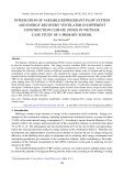
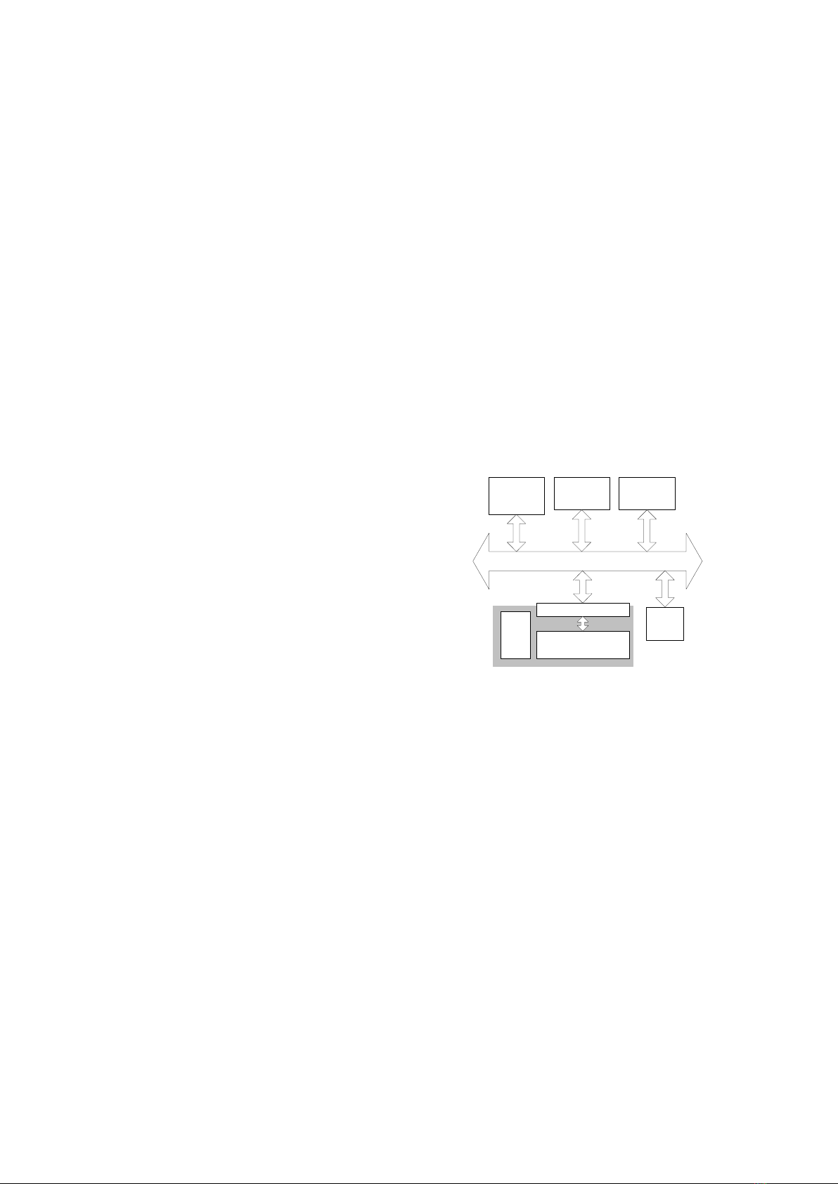
2. MUSRA Architecture
2.1. Architecture Overview
Context
Parser
Context
Memory
Input DMA
Output DMA
Data
Memory
RCA
Crossbar Switch
RC
00
RC
01
RC
07
RC
10
RC
11
RC
17
RC
70
RC
71
RC
77
Crossbar Switch
Crossbar Switch
IN_FIFO
IN_FIFO
GRF
AHB/CGRA Interface
CDMAC
DDMAC
Figure 2. MUSRA architecture.
The MUSRA is composed of a
Reconfigurable Computing Array (RCAs),
Input/Output FIFOs, Global Register File
(GRF), Data/Context memory subsystems, and
DMA (Direct Memory Access) controllers, etc.
(Figure 2). Data/Context memory subsystems
consist of storage blocks and DMA controllers
(i.e. CDMAC and DDMAC). The RCA is an
array of 88 RCs (Reconfigurable Cells) that
can be configured partially to implement
computation-intensive tasks. The input and
output FIFOs are the I/O buffers between the
data memory and the RCA. Each RC can get
the input data from the input FIFO or/and GRF,
and store the results back to the output FIFO.
These FIFOs are all 512-bit in width and 8-row
in depth, and can load/store sixty-four bytes or
thirty-two 16-bit words per cycle. Especially,
the input FIFO can broadcast data to every RC
that has been configured to receive the data
from the input FIFO. This mechanism aims at
exploiting the reusable data between several
iterations. The interconnection between two
neighboring rows of RCs is implemented by a
crossbar switch. Through the crossbar switch,
an RC can get results that come from an
arbitrary RC in the above row of it. The Parser
H.K. NGUYEN et al. / VNU Journal of Science: Comp. Science & Com. Eng., Vol. 31, No. 1 (2015) 1-21
4
decodes the configuration information that has
been read from the Context Memory, and then
generates the control signals that ensure the
execution of RCA accurately and automatically.
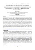
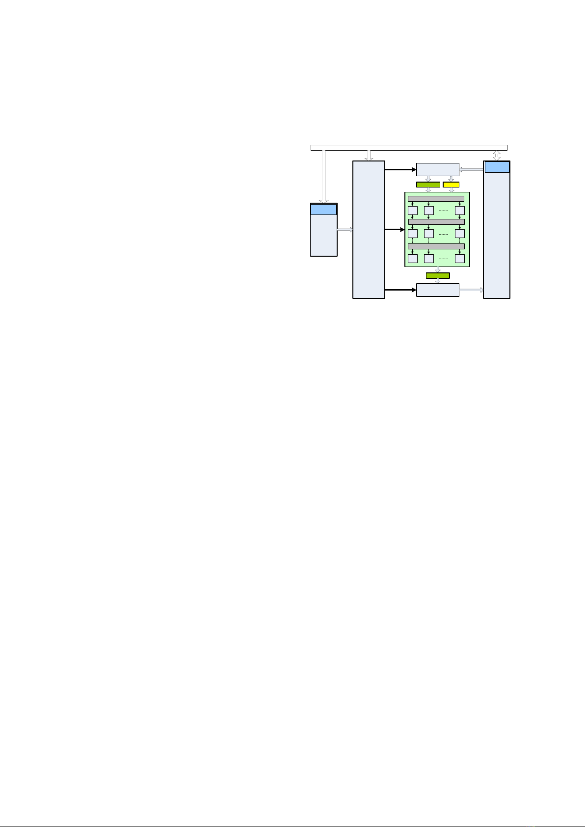
RC (Figure 3) is the basic processing unit of
RCA. Each RC includes a data-path that can
execute signed/unsigned fixed-point 8/16-bit
operations with two/three source operands, such
as arithmetic and logical operations, multiplier,
and multimedia application-specific operations
(e.g. barrel shift, shift and round, absolute
differences, etc.). Each RC also includes a local
register called LOR. This register can be used
either to adjust operating cycles of the pipeline
or to store coefficients when a loop is mapped
onto the RCA. A set of configuration registers,
which stores configuration information for the
RC, is called a layer. Each RC contains two
layers that can operate in the ping-pong fashion
to reduce the configuration time.
DATAPATH
MUX MUX
LOR
MUX
AB
C
MUX
InputFIFO
PRE_LINE
InputFIFO
PRE_LINE
InputFIFO
OUT_REG
LOR_input
LOR_output
PE_OUT
PRE_LINE
LOR_OUT
PE
CLK
RESETN
A_IN B_IN
C_IN
Config._Addr
Config. Data
ENABLE
GRFs
Cnfig.
REGs
Layer
1
Config.
REGs
Layer
0
Config._ENB
Figure 3. RC architecture.
The data processed by RCA are classified
into two types: variables are streamed into the
RCA through the input FIFO meanwhile
constants are fed into the RCA via either GRF
for scalar constants or LOR array for array
constants. The constant type is again classified
into global constants and local constants.
Global constants are determined at compile-
time therefore they are initialized in context
memory of the MUSRA at compile-time and
loaded into GRF/LORs while configuring the
RCA. Local constants (or immediate values) are
not determined at compile-time, but are the
results generated by other tasks at run-time,
therefore, they need to be loaded dynamically
into GRF/LCRs by configuration words.
2.2. Configuration Model
The configuration information for the
MUSRA is organized into the packets called
context. The context specifies a particular
operation of the RCA core (i.e. the operation of
each RC, the interconnection between RCs, the
input source, output location, etc.) as well as the
control parameters that control the operation of
the RCA core. The total length of a context is
128 32-bit words. An application is composed
of one or more contexts that are stored into the
context memory of the MUSRA.
The function of the MUSRA is
reconfigured dynamically in run-time according
to the required hardware tasks. To deal with the
huge configuration overhead in the
reconfigurable hardware, the proposed design
of the MUSRA supports a mechanism to pre-
load and pre-decode the configuration context
from the context memory to the configuration
layers in the RCA. By this method, the
configuration of the MUSRA can take place
behind the execution of the RCA. As a result,
once the RCA finishes calculating with the
current context, it can be immediately changed
into the next context.
2.3. Execution Model
It is a well-known rule of thumb that 90%
of the execution time of a program is spent by
10% of the code of LOOP constructs [9]. These
LOOP constructs are generally identified as
kernel loops. Most of them have computation-
intensive and data-parallel characteristics with
high regularity, so they can be accelerated by
H.K. NGUYEN et al. / VNU Journal of Science: Comp. Science & Com. Eng., Vol. 31, No. 1 (2015) 1-21
5
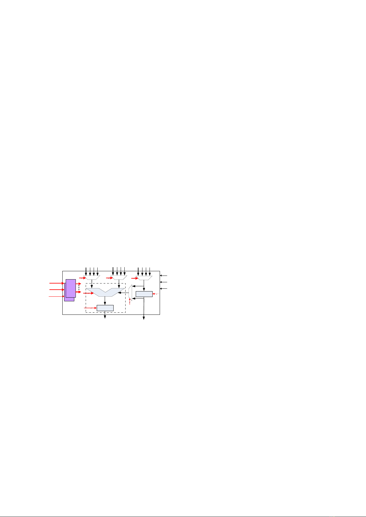
+
&
-
x y
×
CLK1
CLK2
CLK3
CLK4
CLK5
LOAD -
EXECUTION
STORE-
EXECUTION
z
v
InputFIFO
x y
z
LOAD
NI = 2
A
CLK6 w
OutputFIFO
v
w
0
1
Output #1
Output #2
NO = 2
Data broadcasted
directly to every RC
Input #1
Input #2
35
t
t
EXECUTION
(a)
PE
LOR
PE
PE
PE TD
PE
PE
PE LOR
PE TD
xy
×
-
+
&
Stage1
Stage2
Stage3
Stage4
z
LOR
LOR
LOR
LOR
PE TD PE TD
A
Stage4
w
t
GRF(0)
OUT_FIFO(0)
OUT_FIFO(0)
v
(b)
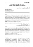
Figure 4. (a) DFG representation of a simple loop body, and (b) its map onto RCA.
hardware circuits. The MUSRA architecture is
basically the such-loop-oriented one. By
mapping the body of the kernel loop onto the
RCA, the RCA just needs configuring one time
for executing multiple times, therefore it can
improve the efficiency of the application
execution. Executing model of the RCA is the
pipelined multi-instruction-multi-data (MIMD)
model. In this model, each RC can be
configured separately to a certain operation, and
each row of RCs corresponds to a stage of a
pipeline. Multiple iterations of a loop are
possible to execute simultaneously in the
pipeline.
For purpose of mapping, a kernel loop is
first analyzed and loop transformed (e.g. loop
unrolling, loop pipelining, loop blocking, etc.)
in order to expose inherent parallelism and data
locality that are then exploited to maximize the
computation performance on the target
architecture. Next, the body of the loop is
represented by data-flow graphs (DFGs) as
shown in Figure 4. Thereafter, DFGs are
mapped onto RCA by generating configuration
information, which relate to binding nodes to
the RCs and edges to the interconnections.
Finally, these DFGs are scheduled in order to
execute automatically on RCA by generating
the corresponding control parameters for the
CGRA’s controller. Once configured for a
certain loop, RCA operates as the hardware
dedicated for this loop. When all iterations of
loop have completed, this loop is removed from
the RCA, and the other loops are mapped onto
the RCA.
The execution of a loop is scheduled so that
the different phases of successive iterations are
overlapped each other as much as possible.
Scheduling also needs to ensure that there are
not any conflicts between resources as multiple
phases take place simultaneously.
Parallel processing increases not only the
computation performance but also the pressure
on the data bandwidth. The system’s bandwidth
is necessary to ensure that data is always
available for all resources running concurrently
without the IDLE state. One way to increase
data availability is to exploit the data locality
that refers to capability of data reuse within a