
TNU Journal of Science and Technology
229(06): 259 - 268
http://jst.tnu.edu.vn 259 Email: jst@tnu.edu.vn
A 551-ns SETTLING TIME OUTPUT CAPACITOR-LESS LDO
WITH PROTECTION CIRCUITS
Nguyen Thanh Long*
Academy of Military Science and Technology
ARTICLE INFO
ABSTRACT
Received:
12/4/2024
This paper proposes an output-capacitorless low-dropout regulator
(OCL-LDO) with simple structure and fast load transient response for
system-on-chip applications. The proposed OCL-LDO does not require
output capacitance and remains stable at no-load condition. A combining
frequency compensation technique is utilized to reduce on-chip
compensation capacitor without degrading loop stability at light load and
improve load transient response speed simultaneously. In addition, over-
temperature, over-voltage, and short-circuit protection functions are also
integrated into the OCL-LDO to ensure circuit safety during operation.
The proposed OCL-LDO regulator has been implemented and simulated
in a 180 nm CMOS process. Simulation results demonstrate the OCL-
LDO regulates the output at 0.9 V from a voltage supply of 1.8 V. The
protection circuits turn off the OCL-LDO when a problem occurs. The
OCL-LDO consumes 71.6 μA quiescent current at light load and can
recover within 655 ns for load transient from 0 to 100 mA and within 551
ns for load transient from 100 mA to 0 in 100 ns. The OCL-LDO obtains
good load regulation of 2.54 µV/mA.
Revised:
31/5/2024
Published:
31/5/2024
KEYWORDS
Low-dropout regulators
Output capacitor-less
Frequency compensation
Protection function
Settling time
MẠCH LDO KHÔNG SỬ DỤNG TỤ ĐIỆN NGOÀI CHIP TÍCH HỢP
CÁC MẠCH BẢO VỆ CÓ THỜI GIAN KHÔI PHỤC 551 ns
Nguyễn Thành Long
Viện Khoa học và Công nghệ Quân sự
THÔNG TIN BÀI BÁO
TÓM TẮT
Ngày nhận bài:
12/4/2024
Bài báo này đề xuất thiết kế mạch ổn áp điện áp rơi thấp không sử dụng
tụ điện tại đầu ra (OCL-LDO) với cấu trúc đơn giản và đáp ứng chuyển
tải nhanh cho các ứng dụng tất cả trên một chip. Mạch OCL-LDO đề
xuất ổn định trong điều kiện tải nhẹ mà không yêu cầu tụ điện tại đầu
ra. Kỹ thuật bù tần số kết hợp được sử dụng để giảm giá trị tụ điện bù
trong chip mà không làm giảm sự ổn định của mạch trong khi cải thiện
được tốc độ đáp ứng chuyển tải. Bên cạnh đó, các chức năng bảo vệ quá
nhiệt, quá dòng, ngắn mạch cũng được tích hợp trong mạch OCL-LDO
để đảm bảo mạch an toàn trong suốt thời gian hoạt động. Mạch ổn áp
OCL-LDO được thiết kế và mô phỏng trên công nghệ CMOS 180 nm.
Kết quả mô phỏng cho thấy mạch OCL-LDO tạo ra điện áp đầu ra ổn
định 0,9 V từ điện áp nguồn cung cấp 1,8 V. Mạch bảo vệ tắt mạch
OCL-LDO khi có sự cố xảy ra. Mạch OCL-LDO tiêu thụ 71,6 µA dòng
tĩnh trong điều kiện tải nhẹ và có thể khôi phục điện áp đầu ra trong 655
ns khi dòng tải thay đổi từ 0 đến 100 mA và trong 551 ns khi dòng tải
thay đổi từ 100 mA về 0 trong 100 ns. Mạch OCL-LDO đạt được điều
chỉnh tải tốt với 2,54 µV/mA.
Ngày hoàn thiện:
31/5/2024
Ngày đăng:
31/5/2024
TỪ KHÓA
Mạch ổn áp
Không sử dụng tụ điện tại đầu ra
Bù tần số
Chức năng bảo vệ
Thời gian khôi phục
DOI: https://doi.org/10.34238/tnu-jst.10136
Email: 34thanhlong@gmail.com

TNU Journal of Science and Technology
229(06): 259 - 268
http://jst.tnu.edu.vn 260 Email: jst@tnu.edu.vn
1. Introduction
The power management ICs are critical modules in today’s system-on-chip Internet-of-
Things, and mobile devices applications. Various types of power management units are required
for widely distributed voltage domains [1]. Low-dropout regulators (LDO) are usually cascaded
after power-efficient switching regulators to filter the switching ripples and provides a regulated
supply voltage [2]. However, excess loading current output, improperly shorting output
terminals, or over temperature will possibly damage the LDO regulator. As a result, design of
LDO is necessary to integrate internal protection functions to improve the stability and safety. So
far there are several researches about protection circuits for LDO [3] – [7]. In which, researches
[3], [4] present principle of current protection, paper [5] illustrates solution to protect voltage and
over-temperature, and researches [6], [7] show architecture of over-temperature and current
protection circuits. However, these studies only focused on the design of protection circuits
without carefully evaluating the quality of LDO circuit when integrated with protection circuits.
Conventional LDOs have an off-chip capacitor in the order of several micro-farads at the
output to stabilize the system [8]. However, using bulky off-chip output capacitors for stability
and the power supply rejection ratio (PSRR) significantly affects the system size. Output
capacitor-less LDO (OCL-LDO) is beneficial to reduce its area and increase the integration
density by removing a bulky external capacitor [9], [10]. However, after getting rid of the large
off-chip capacitor, the pole at the LEO output is no longer dominant and the stability control
becomes more challenging. To overcome this problem, different compensation techniques using
small capacitors (∼pF) have been proposed for OCL-LDOs [11] – [18]. Researches [11], [12]
utilize internal Miller compensation technique to obtain good phase margin (PM) but they have
narrow Gain-Bandwidth (GBW). To improve GBW, researches [13], [14] compensate frequency
by combining capacitor and feedback resistor. Unfortunately, they have poor PM. Researches
[15], [16] use active feedback technique, paper [17] employs feedforward path compensation and
paper [18] utilizes hybrid passive-active frequency compensation to achieve high PM and large
GBM simultaneously. However, they have long settling time (TS), 9 µs in [15], 3.2 µs in [16], 2.2
µs in [17] and 2.6 µs in [18]. To overcome these limitations, research [19] combines internal
Miller compensation, combining capacitor and feedback resistor, and active feedback. It obtains a
short settling time of 0.59 µs. However, these studies have not integrated the protection function
in the LDO circuit.
This paper proposes a OCL-LDO integrating protection circuits inside, including over-
voltage, short-circuit and over-temperature protection. In addition, by using the frequency
compensation technique in [19], the proposed OCL-LCO achieves short settling time. This paper
is organized as follows. Section 2 introduces the detailed design of the the proposed OCL-LDO.
Section 3 shows the experimental results on 180 nm CMOS process followed by conclusions in
Section 4.
2. Design of proposed OCL-LDO
2.1. Frequency compensation technique for OCL-LDO [19]
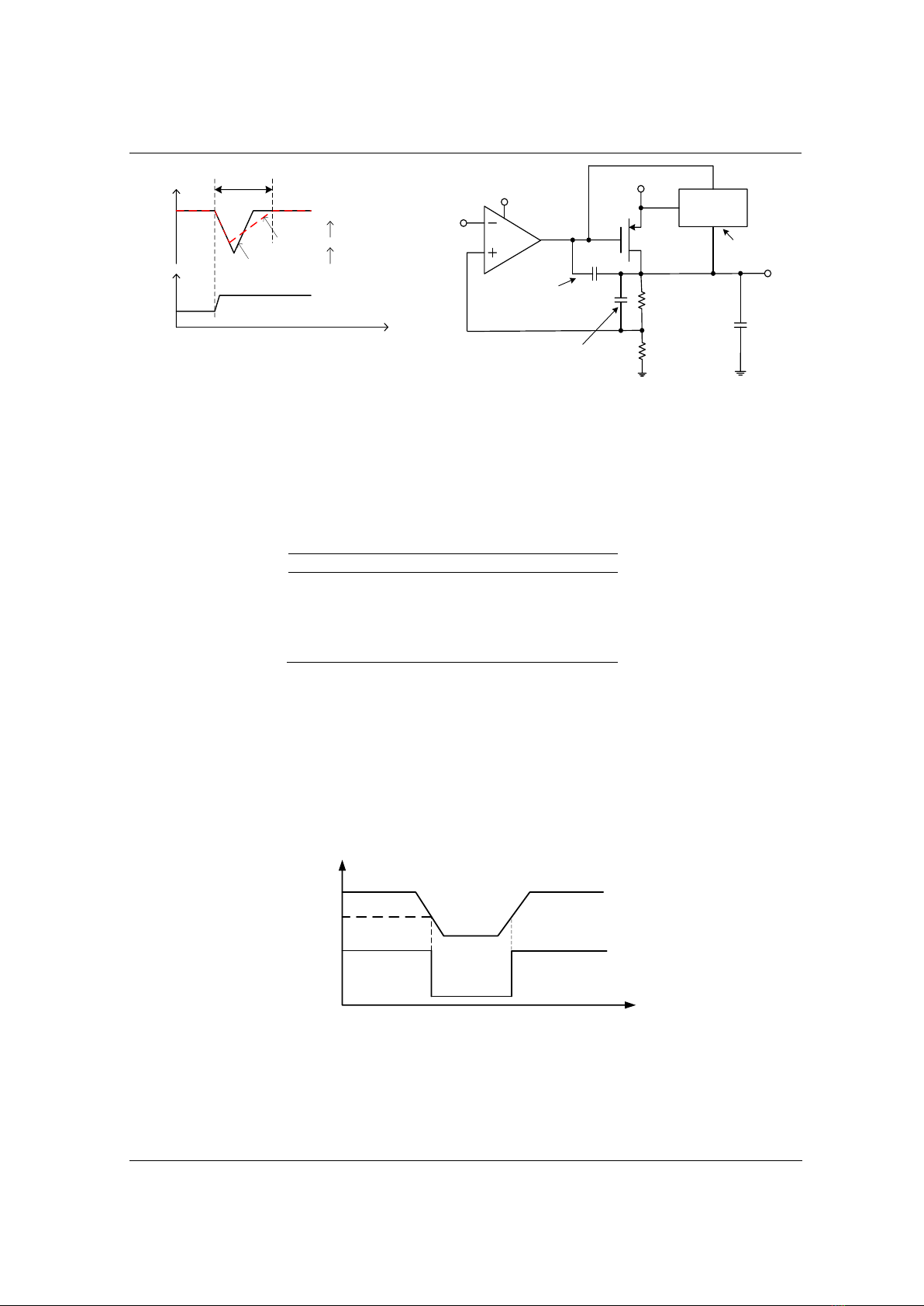
Figure 1 describes the change in output voltage VOUT of OCL-LCO when the load current Iload
changes from low (IL) to high (IH) in two cases GBW1 and GBW2 [20].
When the GBW1 is larger than the GBW2, the TS in case of GBW1 is shorter than that of
GBW2. As a result, GBW is inversely proportional to the TS. As mentioned in [11], the Miller
capacitor (CC) is inversely proportional to the GBW of the system, increasing the CC value will
decrease the GBW value, leading to an increase of TS. Therefore, to reduce TS when the load
current changes, we can rise GBW or fall the CC capacitor value. However, the decreasing CC
means reducing circuit stability. To deal with this problem, research [19] proposed a frequency
compensation architecture as shown in Figure 2.
TNU Journal of Science and Technology
229(06): 259 - 268
http://jst.tnu.edu.vn 261 Email: jst@tnu.edu.vn
ILoad
Vout
TS
GBW1
GBW2
GBW1GBW2
>
t
TS
CC
IL
IH
Figure 1. The block diagram of proposed
wireline receiver
EA
VIN
VRFF
VIN
CC
MP
VOUT
CL
RF1
RF2
CF
Miller
capacitor
Feedback capacitor
AF
Active
feedback
Figure 2. Frequency compensation technique for OCL-LDO
By using three compensation methods simultaneously: internal Miller capacitor, combining
capacitor and feedback resistor, and active feedback, this proposal achieves high DC gain (> 90
dB), good PM (> 600) to ensure stable operation for OCL-LDO while improving GBW. As a
result, the TS decreases. The designed values of capacitors and resistors in OCL-LDO core circuit
are shown in Table 1.
Table 1. Designed parameters of OCL-LDO core circuit
Parameter
Value
CC
5.9 pF
CF
4.5 pF
CL
10 pF
RF1
8 kΩ
RF2
16 kΩ
2.2. Design of protection circuits for OCL-LDO
2.2.1. Design of short-circuit protection circuit
As it has already being mentioned, the LDO output voltage is regulated meaning that it is
constant. If a short-circuit exists, the output voltage will drop to a very low value or even to zero,
suddenly. The protection circuit has to be able to sense these voltage changes, sharply, and
produce a control signal that will tum off the LDO. Thus, the short-circuit protection circuit
protects the LDO from a short-circuit issue on the output, improving the reliability and stability
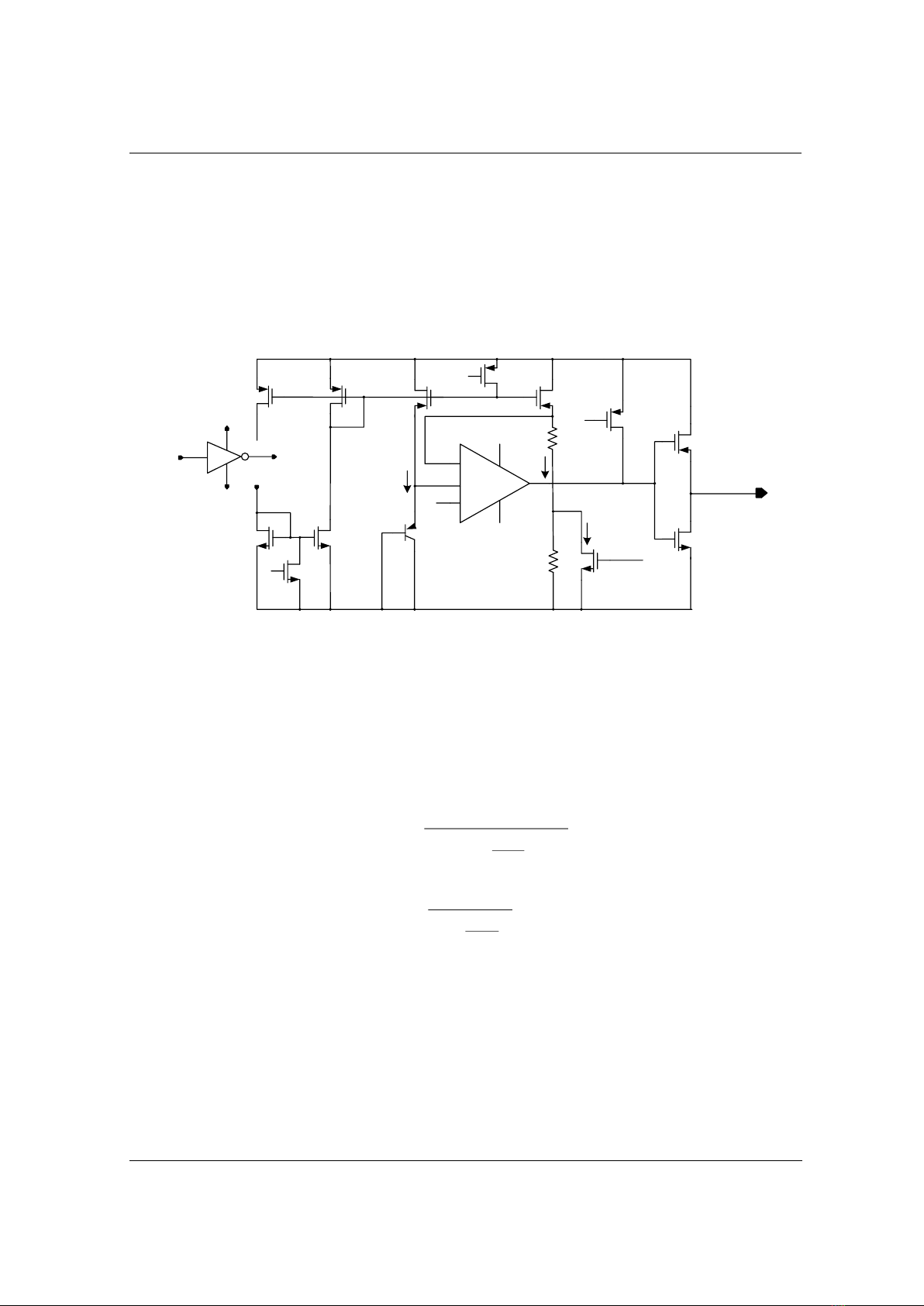
of the system. The operation principle of short-circuit is illustrated in Figure 3.
Vout
SHORT
V
t(s)
33%Vout
Figure 3. Short-circuit protection principle
Short-circuit protection circuit is designed based on a comparator circuit. The comparator will
compare two input signals including an LDO output voltage and a reference voltage. When a
short-circuit issue occurs, the output voltage of the LDO drops suddenly and goes through a
threshold that is 33% output voltage in this paper, then the output signal of the circuit (SHORT)
goes to low logic to turn off the LDO. When the LDO circuit output voltage increases to greater
TNU Journal of Science and Technology
229(06): 259 - 268
http://jst.tnu.edu.vn 262 Email: jst@tnu.edu.vn
than 33% its desired output voltage, the SHORT signal becomes high logic to indicate that the
short-circuit issue has ended.
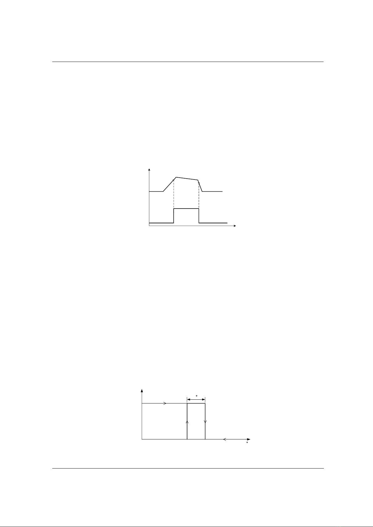
2.2.2. Design of over-voltage protection circuit
LDO provides stable output voltage, ensuring reliable operation of electronic devices. However,
in some cases the output voltage of the LDO increases suddenly, which can damage the electronic
devices powered by the LDO. Therefore, integrating an over-voltage protection circuit (OVP) in the
LDO is very important to limit the output voltage within a safe threshold and avoid unwanted
situations. The design of over-voltage circuit is based on a comparator circuit similar to the short-
circuit protection circuit. When the output voltage exceeds the safe threshold, the protection circuit
will be activated to turn-off the LDO. The LDO will be activated again when the output voltage
returns the safe operation range. Figure 4 demonstrates principle of OVP circuits.
Voltage
105%99.5%
VOUT
OVP t(s)
Figure 4. Over-voltage protection principle
In this paper, the upper thresholds is selected as 105% output voltage. When the output
voltage exceeds 105% its expected value, the LDO will be turned off (OVP signal stays in high
logic), next when the output voltage reaches 99.5%, the protection circuit will turn on the LDO
again (OVP signal stays in low logic).
2.2.3. Design of over-temperature protection circuit
During chip operation, with an increase in ambient temperature or heat accumulation inside
the chip, the temperature inside the chip will keep increasing. Furthermore, the essence of LDO is
to regulate voltage by changing the resistance in the power transistor. So if the input and output
voltages are not equal, all the remaining power will be dissipated as heat in the LDO. This heat
can be significant if we use such a regulator for high load currents. In addition, when the circuit
operates, the power transistor usually has a large size, large current consumption, and large
resistance, so the amount of heat emitted through it is also large. After several periods of
operation, the circuit temperature gradually increases. If too much heat is dissipated without
intervention to reduce the temperature effect on the device, the device may shut down. As a
result, it can reduce the device's life-span. To protect the chip from damage, an overheating
protection circuit (TSD) is designed and widely used in the chip. Figure 5 presents change
characteristics of over-temperature protection circuit.
TSDON
TSDOFF
TSD[V]
t C
20 C
Figure 5. Temperature change characteristics of over-temperature protection circuit
TNU Journal of Science and Technology
229(06): 259 - 268
http://jst.tnu.edu.vn 263 Email: jst@tnu.edu.vn
When the internal temperature of the LDO reaches to the design value of the overheat
protection (1400C in this design), the overheat protection function will activate (TSDON) to turn-
off the LDO. After that, the internal temperature starts to drop when the temperature delay
function is activated, meaning the overheat protection circuit stops working (TSDOFF) until the
temperature drops 200C compared to the LDO turn-off temperature.
The circuit is designed based on the voltage comparison between the (+) and (-) terminal of
the operational amplifier (OPA) circuit as shown in Figure 6. At the anode of the comparator
circuit, a PNP bipolar transistor is connected to detect the temperature change. At the cathode, the
reference voltage is applied to the overheat protection circuit through a voltage divider.
OPA
GND
M3 M4
M1 M2
M5
M6
M7
M8
M9
R1
R2
Q1
VDD
TSD
Vb
VDD
GND
EN
EN
TSD
ENB
EN
VDD
I1
I2
I3
GND
I0P5U
ENB
+
-
Ibias
Ibias
M10
M11
M12
Figure 6. Schematic of over-temperature circuit
The comparator circuit (OPA) is used to compare the voltage produced by the constant current
I2 and the voltage change caused by the temperature-dependent current I1. The temperature-
dependent current is generated by a diode-connected transistor Q1 for absolute temperature.
When temperature increases, the voltage at anode of the OPA grows as well. Since it becomes
larger than the voltage at the cathode, the OPA will generate a high logic signal which passes
through an inverter (M8, M9) to generate a low logic signal (TSD). This signal is applied to the
OCL-LDO core circuit to turn-off the LDO. The shutdown and reset temperatures T1 and T2
respectively are calculated using the formulas [5]:
1 2 2 3 2
1
1
S1
()
ln( )
EB
R R I I R q
TI
kI
+−
=
(1)
1 2 2
2
1
S2
()
ln( )
EB
R R I q
TI
kI
+
=
(2)
In which, R2 and R3 are resistors that create a constant current I2; I3 is the drain current of M7;
I1 is the temperature dependent current; q is the electron charge; k is Boltzmann's constant; IEBS1
and IEBS2 are the emitter–base currents at temperatures T1 and T2, respectively. Equations 1 and 2
reveal that, R2, R3 are adjusted to vary the on/off temperature threshold of TSD circuit.
2.3. Integrating protection circuits into OCL-LDO core circuit
Solution integrating protection circuits into OCL-LDO core circuit is demonstrated in Figure
7. The circuit consists of an NOT gate, a three-input AND gate and a PMOS transistor.


![Chương trình đào tạo cơ bản Năng lượng điện mặt trời mái nhà [mới nhất]](https://cdn.tailieu.vn/images/document/thumbnail/2026/20260126/cristianoronaldo02/135x160/21211769418986.jpg)

![Chương trình đào tạo cơ bản Năng lượng gió [Tối ưu SEO]](https://cdn.tailieu.vn/images/document/thumbnail/2026/20260126/cristianoronaldo02/135x160/53881769418987.jpg)


