ISSN: 2615-9740
JOURNAL OF TECHNICAL EDUCATION SCIENCE
Ho Chi Minh City University of Technology and Education
Website: https://jte.edu.vn
Email: jte@hcmute.edu.vn
JTE, Volume 19, Special Issue 03, 2024
7
Electrical Properties of GaN/Ga2O3 P-N Junction: A TCAD Study
Duyen-Thi Nguyen , Khanh Nguyen , Duc-Minh Truong, Huy-Binh Do*
Ho Chi Minh City University of Technology and Education, Vietnam
*Corresponding author. Email: binhdh@hcmute.edu.vn
ARTICLE INFO
ABSTRACT
Received:
12/10/2023
Ga2O3 and GaN are promising candidates for the fabrication of high-power
semiconductor devices due to their wide range of band gap from 3.0 eV to
4.9 eV. Heterostructure of p-type GaN and n-type Ga2O3 (GaN/Ga2O3 p-
n junction) is expected to have an excellent performance for high-power
semiconductor device applications at high temperature. In this work,
effects of GaN thickness and its doping concentration in GaN/Ga2O3 p-n
junction are studied using (TCAD) simulations, aiming at optimizing the
junction performance. It was found that the current-voltage (IV)
characteristic of the diode decreases as the thickness of GaN layer
increases. To achieve a high current output, the optimized thickness is
determined to be 500 nm. Furthermore, the doping concentration within the
diode strongly influences the output current. The highest current is
obtained for an un-doped GaN sample, and the increase in the doping
concentration leads to a decrease in the obtained current.
Revised:
23/10/2023
Accepted:
24/10/2023
Published:
28/08/2024
KEYWORDS
GaN;
Ga2O3;
P-N junction diode;
Band structure of diodes;
High power semiconductor devices.
Doi: https://doi.org/10.54644/jte.2024.1481
Copyright © JTE. This is an open access article distributed under the terms and conditions of the Creative Commons Attribution-NonCommercial 4.0
International License which permits unrestricted use, distribution, and reproduction in any medium for non-commercial purpose, provided the original work is
properly cited.
1. Introduction
β-Ga2O3 is a potential wide bandgap semiconductor with several potential appications such as power
devices, UV photodetectors, photocatalysts, gas sensors, solar cells, and sometimes works as the
transparent conducting materials in optoelectronic devices [1], [2]. Ga2O3 has gained attention due to its
intriguing properties such as ultra-wide band-gap (4.6 - 4.9 eV), high critical field of 8 MV/cm, high
saturation electron velocity of 2 x 107 cm/s, and high electron mobility up to 200 cm2/Vs at room
temperature [3]. Ga2O3 has an advantage over other wide band-gap materials such as SiC and GaN
because of its low fabrication cost using Czochralski (CZ) [4], floating zone (FZ) or edge-defined film-
fed (EFG) methods [5]. In order to utilize Ga2O3 in high power applications, it is crucial to improve the
Baliga's Figure of Merit (BFOM) in metal-oxide semiconductor field-effect transistors (MOSFETs) [6].
This figure of merit is determined by two key factors: dielectric breakdown (Eox, br) and maximum
surface electric field (ESURF max). Previous study reported the ESURF max values for SiO2 and HfO2 are 1.56
MV/cm and 2.60 MV/cm, respectively [7].
Despite many promising applications in electronic devices, the further development of Ga2O3 are
still limited due to the lack of p-type β-Ga2O3 based materials, which is mainly the massive acceptor
ionization energy, low hole activation efficiency, hole-trapping effect, and self-compensation effects of
cation [8]. On the other hand, large band gap p-type semiconductor can be easily achieved in GaN with
the band gap up to 3.4 eV makingit becomes a potential p-type material for the next generation of
power devices [9]-[15]. Therefore, the combination of β-Ga2O3 and GaN in bipolar devices is expected
to to mitigate the drawbacks of Ga2O3 while leveraging the properties of p-type GaN. S. Leone et al.
grew epitaxial GaN/Ga2O3 heterostructures by MOCVD. A strong oxygen inter-diffusion has been
observed at GaN/Ga2O3 interface leads to reduce the quality of GaN layer [16]. Ga2O3/GaN diode was
reported to be used as a light emitting diode (LED) in Yang Zhao’s study [17]. Deep ultraviolet (UV)
photodiodes based on a heterojunction between β-Ga2O3 and GaN were demonstrated to have the highest
sensitivity to the light with < 260 nm and the response time in the order of milliseconds [18]. Recently,
Ga2O3/NiOx p-n junction was fabricated with extremely high breakdown voltage (8.32 kV) and power
figure-of-merit (13.2 GW/cm2) [19].
ISSN: 2615-9740
JOURNAL OF TECHNICAL EDUCATION SCIENCE
Ho Chi Minh City University of Technology and Education
Website: https://jte.edu.vn
Email: jte@hcmute.edu.vn
JTE, Volume 19, Special Issue 03, 2024
8
This study aims to contribute to the development of a GaN/Ga2O3 diode that can be utilized in high-
power device applications. The simulated device is calibrated against experimental GaN and Ga2O3
diodes, considering the effect of thickness of GaN layer and its doping concentration on the performance
of GaN/Ga2O3 diodes. The band structures of devices are investigated to revial which factors that affect
the properties of GaN/Ga2O3 diode.
2. Methodology and Settings
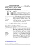
Figure 1. Schematic cross section of GaN/Ga2O3 p-n diode.
Table 1. The details of material parameters of Ga2O3 and GaN used for simulation
Parameters
n-type Ga2O3[7]
p-type GaN*
Band Gap (eV)
4.85
3.43
Eletron Affinity (eV)
3.9
4.31
Effective electron mass
0.28
0.20
Relative dielectric constant
10
8.9
Room-temperature electron mobility (cm2/Vs)
200
-
Room-temperature hole mobility (cm2/Vs)
-
16
Saturation electron velocity (cm/s)
2.00×10⁷
-
Saturation hole velocity (cm/s)
-
1.91×10⁷
*These parameters are default from TCAD.
The GaN/Ga2O3 p-n junction was theoretically studied using the 2-D device simulation tool. The
device structure is illustrated in Fig. 1. All devices have the same n-type doping concentration of 2.6 ×
1018 cm3 in Ga2O3 substrate, and initial p-type doping concentration of 1 × 1019 cm3 in GaN drift layer
was used in the calibration process. To investigate the properties of the diodes, the thicknesses of the
GaN layer were varied at 10 nm, 20 nm, 50 nm, 100 nm, 500 nm and 2 µm. The simulated parameters
of Ga2O3 and GaN are shown in Table 1. In order to consider the impact of carrier concentration and
high electrical field on the mobility, a concentration-dependent lifetime model and a high field model
were used. The Auger recombination model was adapted to consider the influence of high electron
concentration, and a thermal model was used to examine the self-heating effect.
ISSN: 2615-9740
JOURNAL OF TECHNICAL EDUCATION SCIENCE
Ho Chi Minh City University of Technology and Education
Website: https://jte.edu.vn
Email: jte@hcmute.edu.vn
JTE, Volume 19, Special Issue 03, 2024
9
3. Results and Discussion
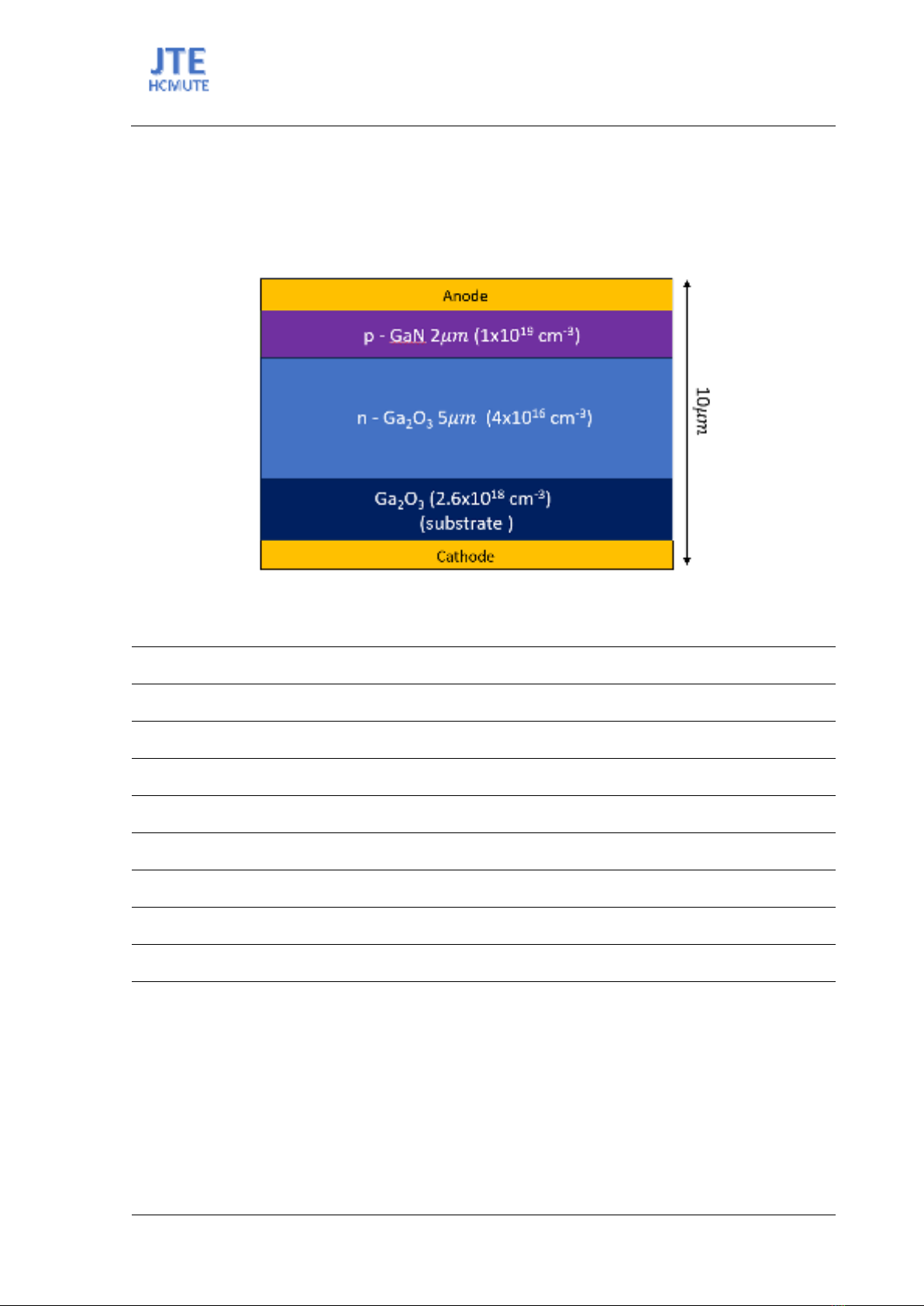
Figure 2. The I-V characteristics of (a) the Ga2O3 diode and (b) the GaN diode as compared to the
experimental results obtained from the same devices [20], [21].
TCAD parameters are calibrated against experimental Ga2O3 and GaN diodes. The I-V
characteristics, which are illustrated in Fig. 2(a) for Ga2O3 diode and in Fig. 2(b) for GaN diode, show
that both I-V curves fit well with the experimental date [20], [21]. The calibrated parameters are used in
simulation of all GaN/Ga2O3 p-n diodes, including the investigation of impacts of GaN drift layer
thickness and the doping concentration of this layer on the behaviors of diodes. The electron mobility
of Ga2O3 was extracted to be 115 cm2/Vs, which is in good agreement with experimental report [22].
Figure 3. Band-diagram of GaN/Ga2O3 p-n junction diode (a) before and (b) after forming the p-n junction
simulated by TCAD.
The band diagram of the GaN/Ga2O3 p-n junction is illustrated in Fig. 3. Before the formation of the
p-n junction, the energy levels of the conduction band (CB) minimum in both GaN and Ga2O3 are nearly
identical. However, a depletion region is observed after the junction region is formed, having a CB offset
of 0.1 eV and a valence band (VB) offset of 1.4 eV. The CB and VB offsets values are consistent with
the findings of a previous report [23].
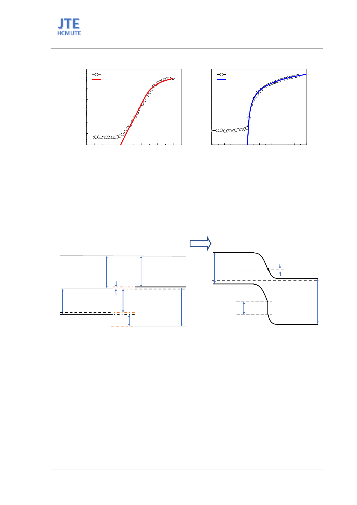
Fig. 4 (a) shows the I-V characteristics of the GaN/Ga2O3 p-n junction as a function of GaN thickness.
It is found that as the thickness of GaN increases the current density decreases because the deleption
region is broadened in the p-type region. However, the reduction in current density is not linear with
respect to the GaN thickness as shown in Fig. 4(b). The threshold voltage of the diode, namely the knee
voltage, is found to decrease significantly for small thicknesses (<100 nm) of GaN, affecting the on-
voltage of the diode significantly. However, as the GaN thickness exceeds 100 nm, the slope of the Kee
voltage – GaN thickness curve decreases, indicating the less dependence of knee voltage on GaN
thickness.
0 1 2 3 4 5 6 7 8
10-2
10-1
100
101
GaN
Current density (A/cm2)
Voltage (V)
Experiment
Simulation
(b)
0.0 0.2 0.4 0.6 0.8 1.0
10-3
10-1
101
103
Current density (A/cm2)
Voltage (V)
Experiment
Simulation
Ga2O3
(a)
GaN ß-Ga2O3
Vacuum level
=4.1 eV Ec= 0.1 eV =4.0 eV
Eg= 3.4eV
Ev= 1.4 eV
Eg= 4.9 eVEFp
EFn
Ev= 1.4 eV
Ec= 0.1 eV
EF
Eg= 3.4eV
Eg= 4.9 eV
GaN ß-Ga2O3
(a) (b)
ISSN: 2615-9740
JOURNAL OF TECHNICAL EDUCATION SCIENCE
Ho Chi Minh City University of Technology and Education
Website: https://jte.edu.vn
Email: jte@hcmute.edu.vn
JTE, Volume 19, Special Issue 03, 2024
10
Figure 4. (a) I-V characteristics of GaN/Ga2O3 p-n junction as a function of GaN thickness, and (b) knee
voltage and current density at Vanode = 5 V as a function of GaN thickness
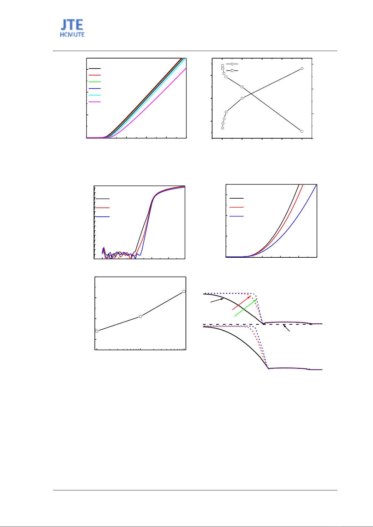
Figure 5. I-V characteristics of GaN/Ga2O3 p-n junction as a function of doping concentration in GaN,
presenting in (a) log scale, and (b) linear scale. (c) Knee voltage as a function of doping concentration in GaN.
(d) Band diagram at GaN/Ga2O3 junction when the doping concentration in GaN is changed from 1.0×1016 cm
3
to 1.0×1018 cm
3.
The impacts of doping concentration of GaN layer on GaN/Ga2O3 p-n junction are investigated in
Fig. 5. We obtained the ratio of Ion/Ioff greater than 1.0×10¹⁵. This high ratio indicates that GaN/Ga2O3
is a highly promising candidate for the applications of high-power devices with low leakage current.
Fig. 5(b) indicates that the current tends to decrease as the doping concentration in GaN increases. This
reduction can be attributed to the changes occurring within the band structure of the diode. Fig. 5(c)
illustrates a slight change in the knee voltage, from 3.54 V to 3.73 V, when the doping concentration is
increased from 1.0×1016 cm−3 to 1.0×1018 cm−3. The electrical properties of the diode can be explained
by simulating their band diagram. Figure 5(d) shows a change in the shape of the GaN/Ga2O3 junction,
varying from a linear-junction (represented by the black solid line) to an abrupt-junction (represented
0500 1000 1500 2000
3.1
3.2
3.3
Knee voltage (V)
Anode current @ 5V
GaN thickness (nm)
Knee voltage (V)
1200
1300
1400
1500
Anode current @ 5V
(b)
2.5 3.0 3.5 4.0 4.5 5.0
0
400
800
1200
Anode current (A/cm2)
Anode voltage (V)
GaN thickness (nm)
10
20
50
100
500
2000
(a)
EF
1.01018 cm3
1.01017 cm3
1.01016 cm3
GaN
Ga2O3
1016 1017 1018
3.5
3.6
3.7
3.8
Knee Voltage (V)
Doping concentration (cm3)
0 1 2 3 4 5
10-12
10-9
10-6
10-3
100
103
Anode current (A/cm2)
Anode voltage (V)
GaN doping conc.
11016 cm3
11017 cm3
11018 cm3
2.5 3.0 3.5 4.0 4.5 5.0
0
400
800
1200 GaN doping conc.
11016 cm3
11017 cm3
11018 cm3
Anode current (A/cm2)
Anode voltage (V)
(a)
(d)
(c)
(b)

ISSN: 2615-9740
JOURNAL OF TECHNICAL EDUCATION SCIENCE
Ho Chi Minh City University of Technology and Education
Website: https://jte.edu.vn
Email: jte@hcmute.edu.vn
JTE, Volume 19, Special Issue 03, 2024
11
by the blue dashed line). This change results in an increase of Schottky barrier within the depletion
region, which explains the decrease of the observed I-V characteristic.
4. Conclusions
In conclusion, the GaN/Ga2O3 p-n junction was investigated using TCAD simulations. The impacts
of GaN thickness and its doping concentration on I-V characteristics of GaN/Ga2O3 diodes was
conducted. It is observed that the knee voltage is strongly dependent on the thickness of GaN when its
thickness is less than 100 nm. The dependence becomes little when the GaN thickness increases. It was
observed that a change in the shape of the GaN/Ga2O3 junction when the doping concentration is
increased from 1.0×1016 cm−3 to 1.0×1018 cm−3, moving from a linear-junction to an arupt-junction. This
change leads to an increase in the Schottky barrier within the depletion region. The study provides
thorough guidance for fabricating GaN/Ga2O3 p-n junction, which is applicable in high power device
applications.
Acknowledgments
This work was funded by the Ho Chi Minh City University of Technology and Education, Vietnam
(Grant No. SV2023-42).
Conflict of Interest
The authors declare no conflict of interest.
REFERENCES
[1] H. von Wenckstern, "Group-III Sesquioxides: Growth, Physical Properties and Devices," Advanced Electronic Materials, vol. 3, p.
1600350, 2017.
[2] S. J. Pearton et al., "A review of Ga2O3 materials, processing, and devices," Applied Physics Reviews, vol. 5, 2018.
[3] J. Yang et al., "Vertical geometry 33.2 A, 4.8 MW cm2 Ga2O3 field-plated Schottky rectifier arrays," Applied Physics Letters, vol. 114,
2019.
[4] Z. Galazka et al., "Scaling-Up of Bulk β-Ga2O3 Single Crystals by the Czochralski Method," ECS Journal of Solid State Science and
Technology, vol. 6, p. Q3007, 2017.
[5] A. Kuramata, K. Koshi, S. Watanabe, Y. Yamaoka, T. Masui, and S. Yamakoshi, "High-quality β-Ga2O3 single crystals grown by edge-
defined film-fed growth," Japanese Journal of Applied Physics, vol. 55, p. 1202A2, 2016.
[6] Z. Cheng, J. Shi, C. Yuan, S. Kim, and S. Graham, "Semiconductors and Semimetals, edited by Y. Zhao and Z. Mi," ed: Elsevier, 2021.
[7] H. B. Do, A. V. P. Gia, V. Q. Nguyen, and M. M. De Souza, "Optimization of normally-off β-Ga2O3 MOSFET with high Ion and
BFOM: A TCAD study," AIP Advances, vol. 12, 2022.
[8] Z. Wu et al., "Energy-driven multi-step structural phase transition mechanism to achieve high-quality p-type nitrogen-doped β-Ga2O3
films," Materials Today Physics, vol. 17, p. 100356, 2021.
[9] H. B. Do, J. Zhou, and M. M. De Souza, "Origins of the Schottky Barrier to a 2DHG in a Au/Ni/GaN/AlGaN/GaN Heterostructure,"
ACS Applied Electronic Materials, vol. 4, pp. 4808-4813, 2022.
[10] J. Zhou, H. B. Do, and M. M. D. Souza, "A new back-to-back graded AlGaN barrier for complementary integration technique based on
GaN/AlGaN/GaN platform," in 2023 7th IEEE Electron Devices Technology & Manufacturing Conference (EDTM), 2023, pp. 1-3.
[11] J. Zhou, H. B. Do, and M. M. De Souza, "Impact of an Underlying 2DEG on the Performance of a p-Channel MOSFET in GaN," ACS
Applied Electronic Materials, vol. 5, pp. 3309-3315, 2023.
[12] D. Kinzer, "GaN power IC technology: Past, present, and future," in 2017 29th International Symposium on Power Semiconductor
Devices and IC's (ISPSD), 2017, pp. 19-24.
[13] L. Zhang et al., "AlGaN/GaN Heterojunction Bipolar Transistors With High Current Gain and Low Specific on-Resistance," IEEE
Transactions on Electron Devices, vol. 69, pp. 6633-6636, 2022.
[14] H. Ohta, N. Kaneda, F. Horikiri, Y. Narita, T. Yoshida, T. Mishima, and T. Nakamura, "Vertical GaN p-n Junction Diodes With High
Breakdown Voltages Over 4 kV," IEEE Electron Device Letters, vol. 36, pp. 1180-1182, 2015.
[15] A. Hickman, R. Chaudhuri, S. J. Bader, K. Nomoto, K. Lee, H. G. Xing, and D. Jena, "High Breakdown Voltage in RF AlN/GaN/AlN
Quantum Well HEMTs," IEEE Electron Device Letters, vol. 40, pp. 1293-1296, 2019.
[16] S. Leone et al., "Epitaxial growth of GaN/Ga2O3 and Ga2O3/GaN heterostructures for novel high electron mobility transistors," Journal
of Crystal Growth, vol. 534, p. 125511, 2020.
[17] H. Wang et al., "Excellent electroluminescence and electrical characteristics from p-CuO/i-Ga2O3/n-GaN light-emitting diode prepared
by magnetron sputtering," Journal of Luminescence, vol. 243, p. 118621, 2022.
[18] S. Nakagomi, T. Sato, Y. Takahashi, and Y. Kokubun, "Deep ultraviolet photodiodes based on the β-Ga2O3/GaN heterojunction,"
Sensors and Actuators A: Physical, vol. 232, pp. 208-213, 2015.
[19] J. Zhang et al., "Ultra-wide bandgap semiconductor Ga2O3 power diodes," Nature Communications, vol. 13, p. 3900, 2022.
[20] I. C. Kizilyalli, A. P. Edwards, O. Aktas, T. Prunty, and D. Bour, "Vertical Power p-n Diodes Based on Bulk GaN," IEEE Transactions
on Electron Devices, vol. 62, pp. 414-422, 2015.
[21] J. Yang, S. Ahn, F. Ren, S. Pearton, S. Jang, J. Kim, and A. Kuramata, "High reverse breakdown voltage Schottky rectifiers without
edge termination on Ga2O3," Applied Physics Letters, vol. 110, 2017.
[22] Y. Kang, K. Krishnaswamy, H. Peelaers, and C. G. Van de Walle, "Fundamental limits on the electron mobility of β-Ga2O3," Journal
of Physics: Condensed Matter, vol. 29, p. 234001, 2017.
[23] P. Li et al., "Construction of GaN/Ga2O3 p–n junction for an extremely high responsivity self-powered UV photodetector," Journal of
Materials Chemistry C, vol. 5, pp. 10562-10570, 2017.