1

VIETNAM ACADEMY

MINISTRY OF EDUCATION AND TRAINING OF SCIENCE AND TECHNOLOGY

GRADUATE UNIVERSITY OF SCIENCE AND TECHNOLOGY --------------------------------------------- Kieu Ngoc Minh FABRICATION OF FLOWER-LIKE, DENDRITE-LIKE NANOSTRUCTURES OF GOLD AND SILVER ON SILICON FOR USE IN THE IDENTIFICATION OF SOME ORGANIC MOLECULES BY SURFACE ENHANCED RAMAN SCATTERING Major: Electronic material Code: 9 44 01 23 SUMMARY OF MATERIAL SCIENCE DOCTORAL THESIS Ha Noi – 2020

2

This thesis was accomplished in: Graduated University of Science and Technology – Vietnam Academy of Science and Technology.

Supervisor: 1. Prof. Dr. Dao Tran Cao 2. Dr. Cao Tuan Anh Peer reviewer 1: Peer reviewer 2: Peer reviewer 3: This thesis will be defended in: The dissertation will be defended in front of the Institute of Doctoral Dissertation Assessment Council, taking place at the Academy of Science and Technology - Vietnam Academy of Science and Technology at ... hour .... ', day ... month ... year 2020 This thesis will be stored in: - Library of Graduated University of Science and Technology - Vietnam National Library

1

Prologue

SERS (surface-enhanced Raman scattering) is a modern analytical technique that is being strongly researched in the world and Vietnam to detection trace (ppm-ppb range) of many different molecules, especially organic and biological molecules. In SERS technique, the most important is the SERS substrate. The SERS substrate is a rugged continuous or discontinuous precious metal (silver or gold) at the nano-scale. When analyte molecules are added to this surface, the signal of Raman scattering of the analyte molecule is greatly enhanced. Thus, it can be said that SERS substrate is the device that amplifies Raman scattering signal of the analyte molecule.

In Vietnam, there are some researches on the fabrication of Ag, Au precious metal nanostructures and using as SERS substrates. However, the researches mainly focus fabricate nanoparticle structures and so far, fabrication of silver nano-dendrites (AgNDs), silver nano-flowers (AgNFs) and gold nano- flowers (AuNFs ) very few, especially the statements on fabrication of these structures on silicon. For the purpose of studying and researching AgNDs, AgNFs and AuNFs materials on silicon as well as the properties and applications of this material, I chose the title of the thesis is “Fabrication of flowers-like, dendrites-like nanostructure of silver and gold on silicon for using in detection some organic molecules by surface enhanced Raman scattering”

In this thesis, we research and fabricate AgNDs, AgNFs, AuNFs structures on silicon by chemical deposition and electrochemical deposition method for the main purpose of using as SERS substrate. To this target, we have studied the morphology, structure and some properties of the nanostructures produced. Then, we use the nanostructures mentioned above as SERS substrates to detect traces of some toxic organic molecules, to test their effectiveness as a SERS substrate.

The scientific significance of the thesis The AgNDs, AgNFs, AuNFs structures on silicon have been two methods of chemical deposition and fabricated by successfully electrochemical deposition with the main purpose for using as SERS substrate. The influence of fabrication parameters on morphology and structure of AgNDs, AgNFs, AuNFs was studied in orderly.

The mechanism of formation of the above structures has been studied. Đã nghiên cứu sử dụng các cấu trúc nano nói trên như là đế SERS để phát hiện một số phân tử hữu cơ độc hại ở nồng độ thấp. These nanostructures have been used as SERS substrates to detect some toxic organic molecules in low concentrations.

2

The thesis includes 4 chapters as follows: This thesis includes of 125

pages (excluding references) with the following layout: Introduction: Presenting the reasons for choosing topic, methods, purposes of researching. Chapter 1: Overview of surface enhanced Raman scattering. Chapter 2: Methods to fabricate and investigate SERS substrates. Chapter 3: Fabrication and investigation of silver and gold nanostructures on silicon. Chapter 4: Using gold, silver nanostructures like flowers and dendrites as SERS substrates to detect traces of some organic molecules. Conclusion: Presenting the conclusions drawn from the research results.

Chapter 1 Overview of surface enhanced Raman scattering

1.1. Raman scattering Raman scattering is inelastic scattering of a photon with material, discovered by Raman and Krishnan in 1928. The frequency of scattering light changes compared to incident light frequency. This amount of change is exactly equal to the oscillation frequency of the matter molecule and does not depend on the frequency of the incident light. So, Raman scattering is specific to each molecule. Raman scattering include of two types: Stockes Raman and anti- Stockes Raman. It should be noted that the intensity of the Raman effect is usually very low (about 10-8 - one hundred million incident photons then one photon is Raman scattering). 1.2. Surface enhanced Raman scattering. Surface enhancement Raman scattering is a phenomenon that when light fly to the analyte molecule adsorbed on the surface of a rugged metal nanostructure, the intensity of the Raman scattering is greatly increased. The metal nanosurface is called SERS substrate. There are two enhancement mechanisms for SERS, which are electromagnetic enhancement mechanism and chemical enhancement mechanism. In which, electromagnetic enhancement mechanism is main contributor. 1.2.1. Electromagnetic enhancement mechanism Surface localized plasmon resonance (LSPR) occurs when the surface plasmon is confined to a nanostruc-ture that Size is smaller than the wavelength of light. From the Fig 1.5, it can see that the electric field of the incident light is an oscillating electric field. In the first half of the cycle, the incident electric field is directed upwards, which has the effect of causing the conduction electrons to move downwards in metal nanoparticles.

3

resulting

dipole field produces (new

Fig 1.5. Schematic illustration of surface localized plasmon resonance (LSPR) with free conducting electrons in metal nanoparticles that are oriented by oscillation due to strong connection with incident light.

presence

light

Fig 1.6. Three different types of chemical enhancement mechanisms in SERS.

Thus, the top part of the metal nanoparticles will be positively charge, the metal nanoparticles becoming an dipole. In the second half of the cycle, the electric field of the incident light changes direction, the dipole also changes direction. As a result, the dipole also oscillates with the frequency of the incident light. The an vibrating light electromagnetic source). If the new electromagnetic field vibrates with the oscillation frequency of the incident light, then we have a resonance. The result, the incident light field is enhanced by E2 times while the scattering field is also enhanced by E2 times, the total field is enhanced by E4 times. 
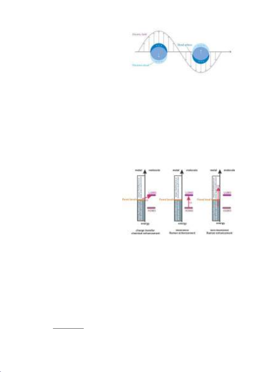
1.2.2. Chemical enhancement mechanism of The chemical Raman with mechanism scattering was observed when plasmonic metals are not used. Studies of non-electromagnetic enhancement mechanisms have shown that resonancing between incident and metal nanostructures can induce charge analyte between transfer molecules and metal. Charge transmission occurs, the metals and molecules of the analyte must be in direct contact with each other. In other words, charge transmission occurs only when the metals and molecules are close enough that the wave functions overlap. The exact mechanism of charge transfer has not been fully understood until now. 1.3. SERS enhancement factor The SERS enhancement factor used in the thesis is the SERS substrate enhancement factor (SSEF) and is calculated by the following formula:

SERS

SSEF

I I

N Normal N

SERS

Normal

4

Fig 1.7. The dependence of SERS enhancement factor on distance of the spherical nanoparticles.

Where, ISERS and INomarl are intensity of Raman spectrum of organic molecule adsorbed on SERS and non-SERS substrate. NNormal, NSERS are the medium number of molecules in the volume scattering (V) of non-SERS measurement, and SERS measurement. 1.4. Dependence of SERS on surface morphology of metal nanostructures Fig.1.7 Simulation dependence of the SERS enhancement factor on the distance between two spherical nanoparticles lying close together. It can be seen that when the distance between the two nanoparticles is 2 nm, the SERS enhancement factor is 108 and the enhancement factor decreased rapidly to only 105 when the distance between the two particles increased to 3 nm. The formation of nanoparticle structures with a narrow between them leading to problems. First, it was difficult to bring the nanoparticles closer together with a distance of 2 nm. Second, analyte molecules into 2 nm gap between particles is also extremely difficult. Therefore, the researchers proceeded to change the shape of the metal nanoparticles in the direction enhancing tips of particles to obtain a strong SERS enhancement. In 2009, P. R. Sajanlal et al demonstrated that SERS enhancement factor of the triangular gold nanoparticle system was 108 (Fig 1.8 a). L. Feng et al fabricated the bow-like silver nanoparticles and the SERS enhancement factor was 109 (Fig 1.8 b). Comparison of SERS enhancement factor obtained from spherical and prism silver nanostructures was also published by S. H. Ciou et al in 2009 (Fig 1.8 (c)). In this comparison, SERS measurements was in solution. The results showed that enhancement factor of the spherical silver nanoparticle was 103, while enhancement factor of the prism- like silver nanoparticle was 105.

Fig 1.8. SEM images of nanoparticles with different shapes: a) gold triangular- like; b) silver bow-like; c) silver prism-like.

5

good

Fig 1.9. SEM image of metal structures: a) Ag-Cu dendrites; b) silver dendrites on an aluminum substrate; c) silver dendrites on a copper substrate and coated with graphene. Dendritic metal structures have tips more than spherical structures. Dendritic structure of precious metals with different shapes was fabricated as shown in Fig 1.9. X. Chen et al fabricated silver - dendrites on a copper substrate and analyzed R6G to a concentration of 10-6 M (Fig 1.9 (a)). Deposition silver on aluminum substrate, then separate the silver dendritic and cover with a layer of gold and identify 1,2-benzenedithiol at a concentration of 10-4 M (Fig 1.9 (b)). L. Hu et al fabricated silver dendrites on a copper substrate, then coated with graphene oxide on top. They demonstrated that for the same analytes, when coated with graphene oxide on top, enhancement factor is 1.2x10⁷ (Fig 1.9 (c)). One of the metal structures SERS for that we enhancement cannot fail to mention are metal structures in shape of flowers (Fig 1.10). H. in 2009 Liang et al successfully fabricated

Fig 1.10. SEM images of metal flowers-like: a) silver nano flower-like; b) gold nano flower-like; c) Gold nano flower-like with holes.

silver flower structures in suspension and used them to detect malachite green with concentrations as low as 10-10 M. Z. Wang et al used electrochemical deposition method to fabricate the gold nanotubes and using this SERS substrate they detected R6G with concentrations as low as 10-10. M. S Ye et al published results for the fabrication of gold nano-structure with holes in the middle and showed that SERS enhancement factor for the biphenyl-4-thiol analyte of this structure was 105. 1.5. Application of SERS During the time since its discovery, SERS has been using as an extremely useful tool for environmental, food, and biomedical analysis. The target molecules analyzed by SERS are also very abundant including pesticides, herbicides, pharmaceutical, chemicals in water, dyes, aromatic chemicals in normal aqueous solutions and in seawater, chlorophenol derivatives and amino acids, war chemicals, soil organic pollutants, and biological molecules such as DNA, RNA. 1.6. Researching of SERS in Vietnam In Vietnam, researching and fabrication on SERS substrates and using of SERS

6

to detect molecules at low concentrations have been starting since 2010. Up to now, in Vietnam, there are several groups has been researching on SERS. Such as, group of GS.VS. Nguyen Van Hieu, Professor's group. Nguyen Quang Liem and Assoc. Ung Thi Dieu Thuy (Institute of Materials Science), Associate's Group. Tran Hong Nhung (Institute of Physics), group of Assoc. Nguyen The Binh (Hanoi University of Science), Assoc. Pham Van Hoi (Institute of Materials Science), group of Professors. Dao Tran Cao (Institute of Materials Science) - this is also the research group that helps me make this thesis. In addition, there are some of other research groups that are also researching on SERS and obtained some good results, we would like to not list here.

Chapter 2 Fabrication and investigation methods of SERS substrate

2.1. Introduction to SERS substrates Currently, there are two types of SERS substrates used SERS substrate is suspension of precious metal nanoparticles (Ag, Ag) inside a certain liquid. SERS substrate is a heterogeneous metal surface. Requirements of a good SERS substrate Strong SERS enhancement factor (> 105). Uniformity on the surface and uniformity between samples (<20%). 2.2. Fabrication methods of SERS substrate There are many ways to classify the fabrication methods of SERS substrates. The most common are: Top-down and bottom-up fabrication. It should also be noted that, approach with any methods, it is possible to fabricate the two types of SERS substrates mentioned above. 2.2.1. Top-down Laser ablation is a way to create a suspension of nanoparticles in solution. Lithography methods, such as electron beam lithography or focused ion beam lithography give metal nanostructures on solid substrates. Advantages: Creates circulating metal structures with variable dimensions and high purity. Not good: It takes a lot of time. The price is expensive because the use of high- tech equipment is necessary. It is difficult to change the surface morphology.

laser ablation E-Lithography The focused ion beam (FIB))

7

2.2.2. Bottom-up There are different methods: - Physical (sputtering, evaporation) - Template, etching - Chemical The chemical reduction method is most used (the metal ion is essentially reduced to atom metal). With the parts in the deposition solution described in the fig include: Reduced substance: usually AgNO3, HAuCl4. Reducing agent (reducing agent): Can be metal, semiconductor, citrate salts, borohydrite (these two salts are most used). Solvent dissolved (most used water, alcohol). Surfactants (most used PVP, CTAB). It should be noted that material can many different roles, for example PVP can make both as a reducing agent and as a surfactant. Deposition can also be performed directly on solid substrates, Al, Cu substrates and in our case Si substrates. Our Si substrate both make as substrate to deposit Ag and Au particles upwards and make as a reducing agent. 2.3. Methods for surveying the structure and properties of SERS substrates SEM imaging: To analyze the morphology of the SERS substrate. X-ray diffraction method (XRD): To analyze the SERS substrate structure. UV-Vis spectrometric method: To analyze plasmon resonance properties of SERS substrate. Raman spectrometric method: To analyze SERS spectrum of toxic organic molecules.

Chapter 3 Fabrication of silver and gold nanostructures on Si 3.1. Fabricating of silver nanostructures on Si by chemical deposition and electrochemical deposition The process of deposition of Ag nanoparticles on Si by chemical deposition method is described as Figure 3.1. After the Si substrates are cleaned, they are soaked in a solution containing the chemicals available. After the fabrication, the substrates are removed, washed and air dry, and measured and analyzed. The process of deposition of Ag nanoparticles on Si by electrochemical deposition method is described in Figure 3.2.

8

Fig 3.1. Schematic of steps for fabricating silver nanostructures on Si by chemical deposition method.

Si on

that

This process is similar to the deposition process of Ag nanoparticles by chemical deposition method. Another after is is fabrication Si substrate attach to the cathode of the DC power, the anode made of platinum.

Fig 3.1. Schematic of steps for fabricating silver nanostructures on Si by electrochemical deposition method.

3.3. Fabrication of silver nanoparticles on Si by chemical deposition method 3.3.1. Fabrication results Figure 3.4 shows SEM images of samples deposited in a solution containing 0.14 M HF and 0.1 mM AgNO3 in water with different deposition times. AgNPs appeared on Si surface at 3 minutes (Figure 3.4 (a)). When the deposition time increased to 4 minutes, the AgNPs were distributed fairly evenly, spherical or ellipsoid with a diameter of about 70 - 100 nm (Figure 3.4 (b)). When the deposition time continued to increase to 5 minutes, the AgNPs tended to clump together and form larger particles (200 - 250 nm) and the distance between particles increased.

Figure 3.4. SEM images of AgNPs on Si by chemical deposition in a solution containing 0.14 M HF / 0.1 mM AgNO3 with deposition time: (a) 3 minutes, (b) 4 minutes and (c) 5 minutes at room temperature. 3.3.2. The mechanism of forming silver nanoparticles on Si that fabricated by chemical deposition method The mechanism for the formation of Ag on Si particles is a galvanic replacement mechanism, in which silver (Ag) replaces Si. Specifically, this process is based

9

on a redox reaction, here, Ag ions in the solution are reduced to atomic silver (Si is reducing agent), while Si is oxidized and dissolved directly following by HF or Si is oxidized by H2O to SiO2, then this SiO2 is dissolved by HF in the solution. Both of these processes occur simultaneously on the Si surface and are represented by the following reaction equations: Cathode:

(3.1)

Anode:

- When Si is oxidized and dissolved directly by HF:

(3.2)

- When Si is oxidized by H2O and dissolved indirectly by HF:

(3.3) (3.4)

- The total reaction for both dissolving Si is:

at

Fig 3.5. SEM images of Ag nanostructures chemically deposited on Si substrates for 15 minutes in 4.8 M HF / AgNO3 solution at room temperature with variable AgNO3 concentration: (a) 0.25 mM, ( b) 1 mM, (c) 2,5 (3.5) Here, it is also important to say more about the role of HF in the deposition solution. Specifically, after the reaction (3.3), SiO2 will gradually form on the Si surface. After a certain time this oxide layer will cover the entire Si surface and it prevents the electron transfer from the Si surface to the Ag + ions and stops the deposition. In order for Ag deposition on Si surface to continue, in the sedimentation solution need more HF and HF will dissolve SiO2 layer according to equation (3.4). Once there are Ag atoms, they will link together to form AgNPs. 3.4. Fabrication of silver nanodendrites structures on Si 3.4.1. Fabrication of silver nanodendrites structures on Si by chemical deposition method Fig 3.5 shows the SEM images of the Si sample surface after being chemically deposited Ag for 15 room minutes a temperature in containing solution and 4.8 M HF the AgNO3 with of concentration AgNO3 changed. It is easy to see that the

10

Fig 3.9. SEM images of AgNDs on Si substrates fabricated by electrochemical deposition of 15 min in a solution of 4.8 M HF / 20 mM AgNO3 with corresponding external potentials: (a) 5; (b) 10, (c) 12 and (d) 15V.

structural morphology mM, (d) 5 mM, (e) 10 mM and (f) 20 mM. of Ag deposited on the Si surface depends on the concentration of AgNO3 in the deposition solution and the AgNDs will also be formed on the Si surface only when the AgNO3 concentration is sufficient. big. Specifically, at a concentration of 20 mM AgNO3 (Fig 3.5 (f)), sub-branches sprouted from Ag nanorods and AgNDs were formed on the surface of Si. It can be seen clearly that the AgNDs structure is a multi-hierarchical structure and that the AgNDs we construct has a quadratic branch structure (a long main branch with short sub-branches growing on either side. ). The diameter of the main branch is about a few hundred nm, and its length is tens of µm, the sub- branches about a few µm long. 3.4.2. Fabrication of Ag nanodendrites on Si by electrochemical deposition method Fig 3.9 shows SEM image of fabricated by AgNDs on Si electrochemical in deposition stable voltage mode with varying potentials (5, 10, 12 and 15V). When the voltage is 12V (Figure 3.9 (c)), now the AgNDs have completely branched to 3 (from the sub-branches to the next ones), creating a pretty and uniform branch structure. . However, when continuing to increase the external voltage to 15V, the structural and order uniformity of AgNDs is now broken and there are some sub- branches that break away from the main branch (Fig 3.9 (d)). It can be seen that when current density increased to 3 mA/cm2, the AgNDs formed on the Si surface were now almost completely branched and began to have quadratic branching, which makes for a density of branches per branch to become very thick (Fig 3.12 (c)). Next, when current density increased to 4 mA/cm2 (Fig. 3.12 (d)), the AgNDs continued to form and overlapped creating an unevenness on the surface. Formation of branch is too thick leading to several small sub-branches to break. The above results show that a deposition current density of 3 mA/cm2 gives the silver foil the most uniformity. The XRD results of the samples after electrochemical deposition (Fig 3.11) show that AgNDs are monocrystalline with a face-centered cubic structure (FCC). The intensity of the peak Ag (111)

11

was much stronger than the other peaks, showing that the AgNDs' growth was mainly in the direction of the crystal plane (111).

(111)

.

) u a (

y t i s n e t n

I

(220)

(200)

20

30

70

50

60

40 2q (Degree)

is

Fig 3.11. XRD diffraction of HaNDs electrochemical deposition on Si.

Fig 3.12. SEM image of AgNDs on Si fabricated by electrochemical substrate deposition for 15 minutes in aqueous solution containing 4.8 M HF/20 mM AgNO3 with the corresponding current densities: (a) 1; (b) 2; (c) 3; and (d) 4 mA/cm2.

3.4.3. Formation mechanism of silver nanodendrites Formation mechanism of AgNDs so far has not been really clarified. However, most researchers believe that the formation of metallic nanotructures can be explained through the Diffusion-limited aggregation (DLA) model and the oriented attachments. According to the DLA model, first there is one particle, then the other particles continuously diffuse towards the original particle to stick together to form the Dendrites shape. Oriented attachments are believed to be particles that, when coming together, somehow rotate the crystal so that the junction has the same crystal orientation to create a single crystal structure. Therefore, the formation mechanism of AgNDs on Si can be explained as follows. First, AgNPs will be formed on Si surface according to the mechanism presented in Section 3.3. Next, other AgNPs will also diffuse continuously towards these original AgNPs to form AgNPs with larger size. AgNPs clusters will attach oriented to form Ag nanorods and nanowires. The nanorods and nanowires will become the main branches (backbone) of the branches. As the main branch grows, new short sub-branches are continuously formed on the main branch, creating a structure resembling fern leaves. More specifically, these sub-branches can also become a major branch to grow shorter sub- branches. This makes the branch structure a multi-hierarchical structure.

12

that when

in

that using of PVP in

Fig 3.15. SEM images of Ag nanostructures chemically deposited on Si in 4,8 M HF/AgNO3/5 mM AsA solution for 10 minutes at room temperature with different AgNO3 concentrations (a) 0.05 mM, (b) 0.1 mM, (c) 0.5 mM and (d) 1 mM.

3.5. Fabrication of the silver nano flower-like structures on Si 3.5.1. Fabrication results It can be seen the concentration of AgNO3 is 1 mM, AgNFs begin to form on the Si surface (Fig 3.15 (d)). AgNFs have relatively uniform sizes (about 700 nm) and their surfaces are rough. According to some authors, the AgNFs can achieve better roughness by adding surfactant polyvinylpyrrolidone (PVP) into deposition solution, so we use PVP replace of AsA the deposition solution fabricate AgNFs on Si. Results in Fig 3.17. It can be the seen deposition solution helps to create the better AgNFs with size of the AgNFs is about 1 µm.

Fig 3.17. SEM images of AgNFs fabricated in 4,8 M HF/1 mM AgNO3/PVP deposition solution with PVP concentration varying (a) 5 mM, (b) 10 mM and (c) 15 mM with 10 minutes at room temperature.

Fig 3.19. SEM images of AgNFs in 4,8 M HF/1 mM AgNO3/10 mM AsA/5 mM PVP deposition solution with different deposition times: (a) 1 minute, (b) 4 minutes, ( c) 10 minutes and (d) 15 minutes. Fig 3.18. SEM images of AgNFs in 4,8 M HF/1 mM AgNO3-/PVP/10 mM AsA deposition solution with different PVP concentrations: (a) 1 mM, (b) 3 mM, (c ) 5 mM and (d) 7 mM with 10 minutes at room temperature.

13

(111)

(200)

) u . a ( y t i s n e t n I

(220)

in to produce

70

40

60

50

30

20

2q (Degree)

Fig 3.20. X-ray diffraction (XRD) of AgNFs on Si

3.5

3.0

2.5

.

AgNPs

2.0

AgNFs

1.5

) u a ( n o i t p r o s b A

1.0

0.5

AgNDs

0.0

600

300

400

700

800

500

region. This

Wavelength (nm)

However, we want AgNFs with sharp points so we used both AsA and PVP in the deposition solution. Results are shown in Fig 3.18. It can be seen that the úing both PVP and AsA deposition helps tips flower-like structure with the size of the AgNFs about 1 µm to 1.5 µm. Our fabrication results also showed that with deposition time 10 minutes, the flower density was the most uniform as illustrated in Fig 3.19. XRD results of the samples after electrochemical deposition (Fig 3.11) show that AgNFs are crystalline with a face-centered cubic structure (FCC). The direction of crystal development is the direction [111]. Fig 3.22 Plasmon resonance spectra of AgNPs, AgNFs, AgNDs structures in the excitation wavelength range from 300 nm to 800 nm. For AgNPs structures of average size 70 nm (Fig. 3.4 (b)) there is a peak at 425 nm excitation wavelength. For AgNFs and AgNDs structures we have a wide plasmon band in the entire excited wavelength broad plasmon band is explained by the Fig 3.22. Plasmon resonance spectra structure AgNFs and AgNDs are of AgNPs, AgNFs, AgNDs structures. multil-branched structures, each of them exhibits its own type of plasmon and is attributed to the hybridization of plasmons relative to the center of the core and sharp vertices around it. Plasmon resonance at longer wavelengths occurs due to a near-field connection between tips when the tips are close together. Due to the heterogeneous size and shape of the core and tip of the AgNDs and AgNFs, the individual plasmon modes of all these sizes and shapes have been coupled together, resulting larger- band. The plasmonic effect is broad and complex as shown in Fig 3.22 and extended to the near infrared band. Plasmon resonance in different excitation wavelength bands of AgNDs and AgNFs structures is also observed when we have recorded SERS spectra of all seven different toxic molecules using both types of steps. Excitation laser wavelength of 633 nm and 785 nm both showed good results. Thus, the characteristic plasmon resonance activity at many

14

different excitation wavelengths is a great advantage over the two structural types AgNDs and AgNFs in SERS analysis. 3.5.2. Formation mechanism of silver flower-like on Si When Si added to the reaction solution containing HF/AgNO3/AsA/PVP, Ag ions are not only reduced by Si (according to reaction equation (3.1)) but also by AsA. The reduction of Ag ions by AsA occurs according to the following reaction equation (2008 Y Wang [169]):

C6H8O6 + 2 Ag+

C6H6O6 + 2 Ag + 2 H+ (3.5) According to Equation (3.5), Ag ions will be reduced directly to Ag atom in solution by AsA. Therefore, Ag deposition in AsA-added solution will occur at a faster rate, leading to size of Ag nano formation on Si surface are larger than the AgNPs deposition in solution only HF and AgNO3. When PVP surfactant is added to the deposition solution, PVP will preferentially adsorb onto {100} surfaces over {111} surfaces. Therefore, developing silver nanostructures, PVP will act as a "capping agent" that prevents the particles from approaching to bond on the {100} surfaces so Ag particles will take precedence. linked to the {111} facets. When the PVP concentration in the deposition was low, the coating of PVP on the (100) surface was low leading to growth at {100} and {111} nearly identical surfaces so the flower had a smooth surface. When the PVP concentration is higher, PVP will cover most of the {100}, resulting in the particles being able to only progress to bonding with the {111} surface and create a tips morphology. Thus, the mechanism of formation of AgNFs in deposition solutions containing AsA and PVP can be divided into three phases: i) First stage: In the presence of the AsA reducing agent, the number of Ag atoms is quickly formed and linked together to form the nucleus. ii) Stage two: Silver atoms continue to be produced and the nuclei develop into nanostructures with larger sizes. iii) Final stage: When nanostructures grow to a certain size, the crystal surfaces become large enough for PVP to be adsorbed on surface. PVP will inhibit the growth of Ag structures in [100] direction and Ag particles will approach the link in [111] direction to create AgNFs structures. 3.6. Fabrication of gold nano flower-like structure by electrochemical deposition method 3.6.1. Fabrication of gold nano flower-like on silver's seed Fabrication of flower-like structures (AuNFs) on Si, we separated nucleation and growth. Specifically, we used Ag nanoparticles fabricated by electrochemical deposition on Si surface as the seed to grow AuNFs. It should be noted further that up to now most research groups have used gold nanoparticles to seed the growth of AuNFs. The reason we use Ag seeds to

15

replace Au seeds is because AgNPs will promote the anisotropic development of Au particles on certain crystal axis, so, the AuNFs structure is more easily formed, it is reported of Ujihara authors group new feature in fabrication of

by

Fig 3.22. SEM images of AuNFs were fabricated electrochemical deposition with current density of 0,1 mA/cm2 for 10 minutes in a solution containing 0.1 mM HAuCl4 and 0.14 mM HF on Si available Ag seed.

Fig 3.21. SEM images of seed of Ag on Si were made by electrochemical deposition with current density of 0,05 mA/cm2 for 3 minutes in solutions containing 0.1 mM AgNO3 and 0.14 mM HF. AuNFs in our study is used of electrochemical deposition in both the seeding and the AuNFs growth step. The SEM results in Fig 3.21 show that after the deposition process, the Ag seeds generated have almost spherical or ellipsoid morphology with an medium size of about 40 nm and distance between AgNPs is about hundreds of nm is formed on the surface Si. Then, we submerged Si substrate with Ag germs in electrochemical solution containing HauCl4. After deposition time, we obtained AuNFs as illustrated in Fig 3.22. SEM image in Fig 3.22 shows that the AuNFs are uniform on the surface with a diameter about 100-120 nm, the distance between AgNFs is about 10 nm. XRD results of AuNFs samples after electrochemical deposition (Fig 3.11) show that AuNFs are crystals with a face-centered cubic structure (FCC). The preferred direction for growing crystals is the direction [111].

Fig 3.23. a) X-ray diffraction (XRD) of gold nano flower-like structure.

3.6.2. Formation mechanism of gold nano flower-like Formation mechanism of gold nano flower-like on Si is based on redox reaction, where, Au3 + is reduced on Si surface (Si as reducing agent) and Si is

16

oxidized to SiO2 (according to the reaction (3.1) to ( 3.5)). The equation for reducing Au3+ to Au atom is represented by the following equation (2011 L M A Monzon [209]):

(3.6) In addition, Au atoms can also be born through an intermediate step according to the equation:

(3.7)

(3.8) Formation of the Au atom according to equation (3.8) there will be an intermediate reduction reaction (equation (3.7)), where, the ions are reduced before being further reduced to gold atom in the equation (3.8). The process of creating gold atom according to equations (3.7) and (3.8) is much weaker than the process of creating a gold atom according to equation (3.6). According to L M A Monzon et al., equations (3.7) and (3.8) would require a greater amount of energy than equation (3.6) or its deposition solvent should be organic solvent instead of H2O. After, Au elements are present, Au will bond with some definite facets of Ag seed. Finally, Au particles will orientately attach to the Au particles already on some surfaces of the Ag seed forming AuNFs.

Chapter 4 Using gold nano flowers-like, silver nano flowers-like, silver nanodendrites structural as SERS substrates to detect traces of some organic molecules 4.1. Reagents are used to analyze SERS and the steps to prepare SERS substrate before measurement Sampling steps for SERS analysis: Preparation of the SERS base (section 3.1); Analytes are premixed with predetermined concentrations (ppm); fixed 25 µl of analyte is applied to SERS substrate surface; spontaneously dry analyte in laboratory environment prior to measuring SERS. There are seven different types of organic molecules that we have used for SERS analysis, including: Paraquat, Pyridaben, Thiram, Crystal violet, Cyanine, Melamine and Rhodamine B. 4.2. Requirements of a good SERS substrate 4.2.1. The uniformity of nano flower-like, dendrites structures of gold and silver In this section we demonstrate the uniformity of SERS substrates fabricated on surface and the uniformity between samples in different fabrications by analyzing SERS via the SERS spectrum of RhB.

17

1506

1355

1527

6000

ṽ ®¬n

1278

1644

619

1196

VT 7

.

) u a (

VT 6

y t i

eliminated most

VT 5

s n e t n

I

VT 4

VT 3

VT 2

VT 1

§(cid:0) tr¾ng

1000

1600

1400

1800

600

800

1200 Raman shift (cm-1)

calculate to

First, we survey the surface uniformity of AgNDs. SERS spectrum of RhB is shown in Figure 4.1. In Fig 4.1, we can see that SERS spectrum of the “substrate with no organic molecules” resembles a line, proving that our sample washing procedure of residue on SERS substrate. As observed in Fig 4.1, the curves and peak intensity at seven different positions are relatively uniform, difficult to observe with the eyes. For more correct results, we perform calculations the repeatability of the measurement using standard deviation SD and the relative standard deviation RSD. Similarly, we calculated for

Fig 4.1. SERS spectra of RhB with 1 ppm concentration obtained when using SERS substrate AgNDs was fabricated by current deposition method at seven different positions.

structures AgNFs and AuNFs, the results are shown in Table 4.5. The results show that the structures mentioned above have good uniformity. Table 4.5. Comparison of data obtained on AgNDs, AuNFs and AgNFs substrates

Type of SERS

SERS peak location

Peak intensity (a.u)

Standard deviation (SD)

Đỉnh 1278

AgNDs AuNFs AgNFs

104.230,213 73.708,814 10.359,4419

10.340,316 5.345,167 719,365

Relative standard deviation (RSD%) 9,920 7,252 6,944

Đỉnh 1644

AgNDs AuNFs AgNFs

93.148,3791 61.130,0398 10.076,8761

10.644,68 5.120,697 807,195

11,428 8,377 8,010

Table 4.6. Data were obtained on AgNFs substrates of five different samples

Analyte concen- tration

SERS peak location

Standard deviation (SD)

five different samples

Peak Intensity (a.u)

Relative standard deviation (RSD%)

Lô 1

12853.24646

1 ppm

Lô 2

12208.44528

1525,680

11,111

Đỉnh 1278 cm-1

Lô 3

12973.93669

18

14738.91166

Lô 4

15883.47427

Lô 5

11704.41479

Lô 1

11416.09864

Lô 2

Lô 3

9

11430.67329

1283,656

10,331

13363.41415

Lô 4

14209.56150

Lô 5

The calculated results for the samples uniformity shown in Table 4.6 are within the permissible range. 4.2.2. Investigation of SERS substrate enhancement factor Table 4.7. Enhancement factor of SERS substrates

Type of SERS

Peak intensity (a.u) (07 peak)

Enhancement factor (EF)

AgNDs

104230,20

AuNFs

73708,81

AgNDs

10538,19

1,04 x 10⁶ 0,69 x 10⁶ 1,05 x 10⁵

The that

The data in Table 4.7 shows that, the SERS substrate reinforcement coefficient of AgNDs substrate is 1,04 x 10⁶, that of AuNFs substrate is 0,69 x 10⁶ and that of AgNF substrates is 1,05 x 10⁵. These numbers show that , SERS substrates have been fabricated to satisfy enhancement factor requirement of a good SERS substrate. 4.3. Application of silver nano-dendrites 4.3.1. Detection of paraquat herbicide It is one of the most widely used herbicides. It is non-selective, killing green plant tissue on contact. Most patients with paraquat poisoning are severe and the mortality rate is very high, estimated at 73%. So the detection of paraquat by SERS is low significant. paraquat concentration the AgNDs@Si substrate can detect is 0.01 ppm. Meanwhile, this limit is 5 ppm for AgNDs @ Si substrates fabricated by chemical deposition (Figure 4.8). Fig 4.8. SERS spectrum of paraquat with different concentrations: (1) 1 ppm; (2) 0, 5 ppm; (3) 0.1 ppm; (4) 0.01 ppm

19

4.3.2. Phát hiện thuốc trừ sâu pyridaben 4.3.2. Detection of pyridaben In Vietnam, pyridaben insecticide is widely used on tea plants to destroy red spiders. Many tea shipments have been returned due to pyridaben concentrations exceeding the permitted threshold. It can be seen that SERS spectrum of pyridabene is very complex and we are also one of the first groups to record the SERS spectrum of pyridabene (Fig 4.9). We also analyzed the SERS spectrum of pyridabene in the commercial product marketed as Koben 15EC (Fig 4.11). Although their SERS spectrum is not as beautiful as SERS spectrum of standard substance. However, we have analyzed pyridaben concentration in Koben 15EC as low as 0.1 ppm.

635

1245

1265

709

1218

1482

1648

1280

1106

1200

670

811

756

1138

780

1615

925

846

944

100 ppm

) u . a ( y t i s n e t n I

) u . a ( y t i s n e t n

I

100 ppm

10 ppm

10 ppm

1 ppm

1 ppm

0.1 ppm

0,1 ppm

600

800

1600

1800

1000

1000 ppm trªn ®(cid:0) Si

600

800

1000

1200

1400

1600

1800

1200 1400 Raman shift (cm-1) 4.11. SERS

spectrum

-1

)

Fig of pyridaben in the insecticide Koben 15EC with different concentrations: 100, 10, 1 and 0.1 ppm

5000 pcs

1386

.

) u a (

y t i s n e t n

I

560

1440

1150

1517

344

446

928

shows 4.12

diluted

100 ppm 10 ppm 1 ppm 0.1 ppm 0.01 ppm

400

600

800

1000

1200

1400

1600

Raman shift (cm-1)

Raman shift (cm Fig 4.9. SERS spectra of pyridabene with different concentrations: 100, 10, 1 and 0.1 ppm 4.3.3. Detection of thiram Thiram recognized were a fungicide Pro- commercial Thiram 80WG (containing the active ingredient thiram at a concentration of 80% by weight), manufactured by Taminco BVBA (Belgium). Fig SERS spectrum of the Pro-Thiram with fungicide deionized water to reach a thiram concentration from 100 ppm to 0.01 ppm (4,2 x 10⁻⁴ M to 4,2 x 10⁻⁸ M)

Fig 4.12. SERS spectra of thiram at different concentrations from 100 ppm to 0.01

20

10000

1618

9000

1375

1174

8000

437

7000

6000

10 ppm

800 913

5000

because residues

4000

3000

1 ppm

) u . a ( y t i s n e t n

I

2000

0.1 ppm

1000

0

-1000

0.01 ppm x 2

-2000

-3000

600

400

800

1800

1600

1400

1200

1000

Raman shift (cm-1) Fig 4.14. SERS spectrum of CV molecule

675

a

982

579

Melamine bét

682

) u . a ( y t i s n e t n

I

foods

575

980

5 ppm 0,5 ppm 0,1 ppm 0,05 ppm 0,01 ppm

1000

1100

1200

600

700

800 900 Raman shift (cm-1)

Fig 4.15. Raman spectra of melamine powder and SERS spectrum of melamine at different concentrations from 0.01 to 5 ppm

in

ppm a

4.4. Application of silver and gold nano flower-like 4.4.1. Detection of violet crystals Containers of seafood products exported from Vietnam rejected in Europe and the US market in recent years of antibiotics are not uncommon. This has a great impact on the seafood export industry and the lives of people working in our country. Crystal violet (CV) is one of the substances mentioned banned above. We analyzed CV at 0.1 ppm concentration. 4.4.2. Detection of melamine In fact, the nitrogen in melamine is a non-protein, that is, it is not a protein but only protein imitation, so it has no nutritional effects like protein. Because of its high nitrogen content, melamine is introduced by into "cheating" manufacturers. Melamine is used to "trick" test method, deceive the examination agencies and of course deceive consumers. Thus, identification of melamine has an important effect in monitoring and monitoring manufacturers when they include them food. We detected melamine with a concentration of 0.01 SERS and enhancement factor of 4,306 x 106. 4.4.3. Detection of xyanide (KCN) Cyanide is present in industrial and municipal wastes, the most abundant source of cyanide pollution is from electroplating, metallurgy, steel processing, gold ore mining and oil-gas industries. The reasons above indicate the urgent need to control cyanide concentrations in water and in soil. This is especially true in Vietnam after the death of a number of fish in the central coast of Vietnam in April 2016.

21

(1)

30000

(1)

25000

25000

(1) - 5 ppm

20000

(2) - 1 ppm

(2)

(2)

(3) - 0,5 ppm

20000

.

(1) - 5 ppm (2) - 1 ppm (3) - 0.5 ppm (4) - 0.1 ppm (5) - 0.05 ppm (6) - 0.01 ppm (7) - 0.005 ppm

(4) - 0,1 ppm

(3)

15000

(3)

(5) - 0,05 ppm

15000

(4)

) u a ( y t i s n e t n I

(4)

) u . a ( y t i s n e t n I

10000

10000

(5)

(5)

(6)

5000

5000

(7)

0 1800

1900

2000

2300

2400

2500

2600

0 1800

2600

2400

2500

2000

1900

2200 2100 Raman shift (cm-1)

Fig 4.17. SERS spectrum of cyanide in ethanol with different concentrations.

towards higher wavelengths. At to elongate. tends that

2100 2200 2300 Raman shift (cm-1) Fig 4.18. SERS spectrum of cyanide in water with different concentrations The results of SERS signals of cyanide in ethanol are show in Fig 4.17. It can be seen clearly that KCN has a single peak at 2105 cm-1, which is attributed to CN bond. Things will be different when KCN is dissolved in water (Fig 4.18). There is now a peak at 2105 cm-1 but the spectrum leg is extended forward. As KCN concentration drops lower, shoulder of spectrum becomes more pronounced, then new-spectral peak is gradually divided into two separate peaks, one peak at 2105 cm-1 and the other at 2140 cm-1. The peak at 2140 cm-1 appears very clearly when the cyanide concentration reducing to 0.01 ppm. We identified that change in shape of the spectral peak at 2105 cm-1 in Fig 4.18 compared to Fig 4.17 is due to the cyanide of silver on the SERS substrate, this process occurs when KCN dissolved in water (instead of ethanol). The orderly variation of SERS spectrum of KCN as its concentration changes as shown in Fig 4.18 can be explained, noting that only cyanide (CN) ions in contact with silver are capable of forming complex with silver. At high cyanide concentrations, the ratio of [Ag(CN)2]- ions low exposure to silver hence the 2105 cm-1 peak of the bond (CN) - remains dominant with the spectral base low IZ concentrations, the percentage of cyanide ions in contact with silver increases with the peak intensity at 2105 cm-1 decreasing continuously, while the peak at 2140 cm-1 appears and gradually becomes separate as shown in Fig 4.18. Thus, by SERS spectrum, for the first time, we observed the complex formation of Ag with cyanide in water.

22

5000 cps

1644

1504

619

1525

1355

1278

1196

5 ppm

colors

1 ppm

0.5 ppm

) u . a ( y t i s n e t n I

0.1 ppm 0.05 ppm

0.01 ppm 1 ppb

0.1 ppb

800

600

1600

1000

1200

1800

and

1400 Raman shift (cm-1) Fig 4.19. SERS spectrum of rhodamine B with different concentrations from 0.1 ppb to 5ppm

4.4.3. Detection of rhodamine B In the process of food processing, to give food a beautiful color industrial colorants are used. Industrial in general, rhodamine B (RhB) in particular are toxic, banned in food because they are difficult to decompose, on the other hand, they also affect the liver, kidneys or long-term residues, cause muscle damage human body, especially can cause cancer. In Vietnam, it is added to products such as squash and melon. We analyzed RhB at as low as 0.1 ppb of concentrations.

Conclusion 1. Successfully fabricated the structures of AgNDs, AgNFs and AuNFs on Si by chemical deposition and/or electrochemical deposition method with controllable of morphological and structural parameters. The new contributions are: - AgNDs with best branching structure (3 branches) were fabricated

by electrochemical deposition in constant current mode.

- The AgNFs were fabricated by chemical deposition with control of the sharpness of petals by AsA and PVP.

- AuNFs were fabricated by electrochemical deposition method from seed, with special feature that seeds are silver nanoparticles (other authors used gold seeds).

2. The main purpose of the fabrication of nanostructures is using them as SERS substrates to detect residues in the trace concentrations of pesticides, toxic additives ... that may be present in food, drinking water, environment ... To test the activity of the above-mentioned nanostructures in the role of SERS substrates, they used to detect trace of some organic molecules. - AgNDs used to detect herbicide paraquat (PQ), thiram insecticide (TR) and pyridaben insecticide (PB) with PQ and TR being detected to 0.01 concentration of ppm. PB can be detected as low as 0.1 ppm. It should be added that our team was the first group to publish PB's SERS spectrum.

- AgNFs used to detect traces of organic pigments contemporary was fungicides crystal violet (CV), food additives melamine (MLM)

23

and toxins or toxics in water as cyanide (CN), with the result of CV and MLM can be detected as low as 0.01 ppm, and CN as low as 5 ppb of concentrations.

- AuNFs to detect traces of rhodamine B (RhB), with the result RhB

results demonstrate that

detected can be to 0,1 ppb. The above SERS spectroscopy the nanostructures fabricated can be used as highly efficient SERS substrates.

3. The above nanostructures tested and evaluated according to the criteria of a good SERS substrate, including hight SERS enhancement factor (>105), uniformity of SERS signals at different points on a good SERS substrate is good (difference <20%), repeatability between different SERS substrates (difference <20%) ... The results show that AgNDs structure has best SERS enhancement factor (~ 106), while AgNFs and AuNFs structures had better uniformity on one substrate and epeatability between different SERS substrates was better than AgNDs, however even for AgNDs there was a relative standard deviation on one sole and between different substrate should not exceed 12%.

LIST PUBLISHED WORKS OF THE THESIS

1. Tran Cao Dao, Truc Quynh Ngan Luong, Tuan Anh Cao, Ngoc Minh Kieu and Van Vu Le, Application of silver nanodendrites deposited on silicon in SERS technique forthe trace analysis of paraquat, Adv. Nat. Sci.: Nanosci. Nanotechnol, 2016, 7, 015007.

2. Kieu Ngoc Minh, Cao Tuan Anh, Luong Truc Quynh Ngan, Le Van Vu, Dao Tran Cao, Synthesis of Flower-like Silver Nanostructures on Silicon and Their Application in Surface-enhanced Raman Scattering, Communications in Physics, 2016, 26, 241-246.

3. Luong Truc Quynh Ngan, Kieu Ngoc Minh, Dao Tran Cao, Cao Tuan Anh & Le Van Vu, Synthesis of Silver Nanodendrites on Silicon and Its Application for the Trace Detection of Pyridaben Pesticide Using Surface Enhanced Raman Spectroscopy, J. Electron. Mater, 2017, 46, 3770-3775.

4. Ngoc Minh Kieu, Tran Cao Dao, Tuan Anh Cao, Van Vu Le and Truc Quynh Ngan Luong, Fabrication of silver flower-like microstructures on silicon and their use as surface-enhanced raman scatering substrates to detect melamine traces, The 6th Asian Symposium on Advanced Materials: Chemistry, Physics & Biomedicine of Functional and Novel Materials (ASAM-6), September 27-30, 2017, Hanoi, Vietnam.

24

5. Tran Cao Dao, Ngoc Minh Kieu, Truc Quynh Ngan Luong, Tuan Anh Cao, Ngoc Hai Nguyen and Van Vu Le, Modifcation of the SERS spectrum ofcyanide traces due to complex formation between cyanide and silver, Adv. Nat. Sci.: Nanosci. Nanotechnol, 2018,9, 025006-5. 6. Tran Cao Dao, Truc Quynh Ngan Luong, Tuan Anh Cao and Ngoc Minh Kieu, High-sensitive SERS detection of thiram with silver nanodendrites substrate, Adv. Nat. Sci.: Nanosci. Nanotechnol, 2019, 10, 025012 (4pp).

7. Tran Cao Dao, Ngan Truc-Quynh Luong, Tuan Anh Cao, Ngoc Minh Kieu, Ngoc Hai Nguyen, Van Vu Le, Electrochemical synthesis of flower-like gold nanoparticles for SERS application, J. Electron. Mater, 2019, 48, 5328-5332.