
TẠP CHÍ KHOA HỌC VÀ CÔNG NGHỆ, Trường Đại học Khoa học, ĐH Huế
Tập 24, Số 1 (2024)
13
REAR-SIDE INTERFACIAL MODIFICATION OF µC-SI:H(N+) BACK SURFACE
FIELD LAYERBY CONTROLLING ITS CRYSTALINE FOR SILICON
HETEROJUNCTION SOLAR CELL APPLICATIONS
Chi-Hieu Nguyen1, Truong-Tho Nguyen2, Ngoc-Toan Dang3,4,
Thanh-Thuy Trinh5,6,*, Vinh-Ai Dao7,*
1 Power Engineering Consulting Company, Southern Power Corporation,
Ho Chi Minh City, Vietnam
2 Faculty of Electronics, Electrical Engineering and Material Technology,
University of Sciences, Hue University, Vietnam
3 Institute of Research and Development, Duy Tan University,Danang, Vietnam
4 Faculty of Environmental and Natural Sciences, Duy Tan University, Danang, Vietnam
5 Department of Physics, International University, Ho Chi Minh City, Vietnam
6 VietnamNational University, Ho Chi Minh City, Vietnam
7 Department of Physics, Faculty of Applied Sciences,
HCMC University of Technology and Education, Ho Chi Minh City, Vietnam
*Email: daovinhai@hcmute.edu.vn, tttrinh@hcmiu.edu.vn
Received: 12/6/2024; Received in revised form: 13/6/2024; Accepted: 24/6/2024
ABSTRACT
In hydrogenated amorphous silicon/crystalline silicon (a-Si:H/c-Si) heterojunction
(HJ) solar cell, the high contact resistance or high Schottky barrier at the back-surface
field (BSF)/Indium Tin Oxide (ITO) is prejudicial to the majority carrier collections
process, as it degrades the fill factor (FF), which in turn, cell efficiency. To minimize
the contact resistance or Schottky barrier, high conductivity of the BSF layer is thus
required. In this study, to preserve high BSF conductivity, while without prompting
silicon dehydrate-related structural defects within the films, the high conductivity
n-type hydrogenated microcrystalline Si layer (c-Si:H(n+)), instead of standard n-
type hydrogenated amorphous silicon, was employed as a BSF layer. The film
conductivity (
d) of the c-Si:H(n+) layer was improved from 0.16 (S/cm) to 4.16
(S/cm), as the crystalline fraction (Xc) increased from 6% to 89%. It was found that
the FF tends depend on the contact resistance at the c-Si:H(n+)/ITO interface, in
defiance of Schottky contact behavior. Thus, series contact resistance dominates the
FF of the device; this finding is opposite to previous report. Using a moderated

Rear-side interfacial modification of µc-Si:H(n+) back surface field layerby controlling its crystaline…
14
crystalline fraction of 60% c-Si:H(n+)-BSF, the photovoltaic parameter of the a-
Si:H/c-Si HJ solar cells yielded an open-circuit voltage of up to 700 mV, in turn giving
an efficiency >20%.
Keywords: passivation, back-surface field, heterojunction, silicon solar cell, µc-
Si:H(n+).
1. INTRODUCTION
Currently, industrial solar cell technology tends toward thinner wafers, thus,
hydrogenated amorphous silicon/crystal silicon (a-Si:H/c-Si) heterojunction (HJ) solar
cells are a focus of interest due to their low-temperature production process (~200C)
and high efficiency of 25.1% [1]. This low-temperature process enables use of
inexpensive, low-quality wafers and reduces the probability of wafer bowing and
breakage [2]. One of the well-known criterion factors for the high performances of a-Si:H/c-
Si HJ solar cells is an excellent surface passivation at the a-Si:H/c-Si heterointerface by
using an intrinsic hydrogenated amorphous silicon (a-Si:H(i)) passivated layer [3].
In addition, to produce high-performance a-Si:H/c-Si HJ devices, the front- and
back-inverted Schottky junction and/or contact resistance should also be minimized [4].
At the back-surface field (BSF)/Indium Tin Oxide (ITO), to promote carrier collections,
an inverted Schottky junction, which is formed due to the work-function discrepancy between
the ITO and the BSF layer must be minimized [5]. To reduce this inverted Schottky junction,
the conductivity of the BSF must be sufficient high to preserve a flat band at the BSF/ITO
interface [6]. Generally, high conductivity is realized by using the high doping
concentration. This increased dopant, however, leads to structural defects within the
film, as a result the open-circuit voltage (Voc) and the fill factor (FF) of the devices are
reduced, as mentioned elsewhere [7]. To compromise between the structural defects and
the conductivity within the films, the stacked-configuration was implementation for the
emitter [8] and also for the BSF layer [7]. This realization shown potential high Voc and
FF as well, compared to standard-configuration. The improvement in Voc and FF was
ascribed to not only the improved a-Si:H/c-Si interface passivation, owing to low doped
layer, which served as a passivated layer, in the stacked-configuration, but also high
conductivity, owing to the high doped layer, which served as a contacted layer to the
ITO, in the stacked-configuration [8]. On the other hand, Ghafarokhi et al., suggested to
improve the electrical conductivity of the emitter via the evolution of the film
crystallinity, which obtained by increasing film thickness. This advance could lead to a
lower Schottky barrier [9]. The lower Schottky barrier height may promote carrier
collection more efficienctly, hence, FF will be improved; nevertheless, this thicker emitter
(p-type c-Si) could cause higher photon absorption, and consequently lower short-circuit
current density (Jsc). Thus, although there has been research studying the optimization of

TẠP CHÍ KHOA HỌC VÀ CÔNG NGHỆ, Trường Đại học Khoa học, ĐH Huế
Tập 24, Số 1 (2024)
15
the emitter layer to achieve low contact resistance and/or Schottky barrier, similar work
for ITO/BSF interface has not been extensively carried out, beside S. Martín de Nicolás
et al. [7] and T. Watahiki et al. [10].
For the aim of obtaining a high conductivity of the film, less detrimental influence
of the a-Si:H/c-Si heterointerface, while without introducing structural defects, within
the film, especially, without detrimental influence influence of the Jsc of the devices, an
approach that is similar to Ghafarokhi et al., was realized in this study, except the doped
layer we used in our study is of n-type c-Si, which is used as a BSF in the BSF/ITO
heterointerface. With this advancement, the Voc and FF of the device showed
improvement, while it did not adversely affect the Jsc.
2. EXPERIMENTAL DETAILS
Czochralski-grown n-type c-Si [CZ c-Si(n)] wafers (1 – 10 cm, 525 m thick,
<100> oriented) were used as an absorber material. To remove organic and inorganic
residues, the wafers were first treated in sequentially with acetone, methanol, de-ionized
water, and RCA (1, 2). Immediately before loading into the chamber, the wafers were
immersed in 1% hydrofluoric acid for 1 min to remove natural native oxide. At the front-
surface of the wafers, the a-Si:H(i) and then p-type a-Si:H (a-Si:H(p)) layers were
deposited in sequence. At the rear-surface, the a-Si:H(i) layer and c-Si:H(n+)-BSF, have
different crystallinity, were deposited. The thickness of the a-Si:H(i), a-Si:H(p) layers
were fixed at 5 and 7 nm, respectively, while the thickness of the c-Si:H(n+)-BSF was
varied to alter film crystallinity. A sputtered ITO layer, 80 5 nm thick and 0.6 0.6 cm
in dimensions, was formed by placing a metal mask directly on the a-Si:H(p) surface.
Finally, Al/Ag electrodes were formed as fingers by thermal evaporation, while the
entire rear-surface was covered with ITO/Al as a back-contact. A schematic diagram of
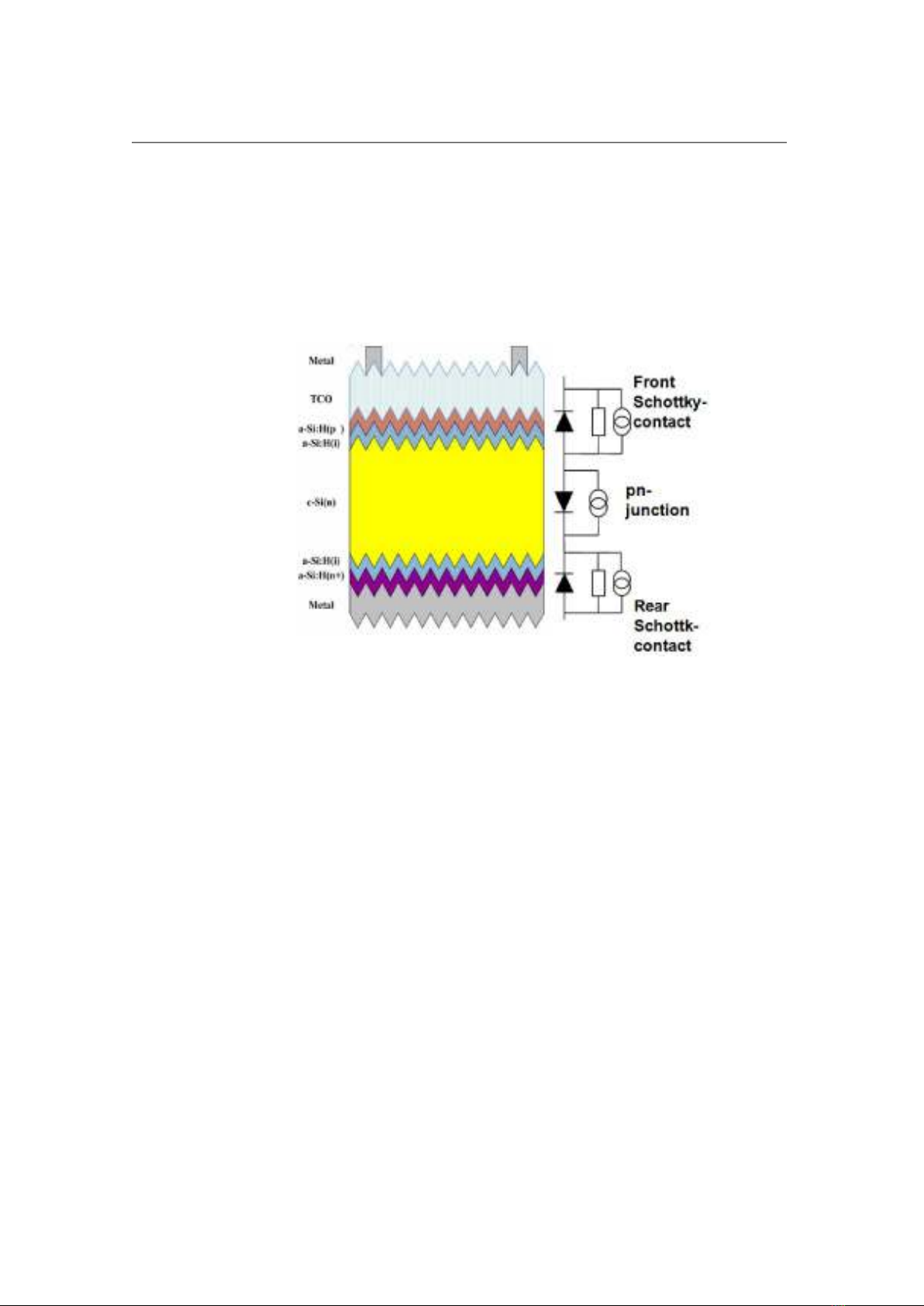
the a-Si:H/c-Si heterojunction solar cell is shown in Fig. 1.
Film thickness was measured using spectroscopic ellipsometry (VASE, J. A.
Woollam, 240 nm < < 1700 nm) at room temperature. Then, the optical constant of each
layer was deduced using the Tauc-Lorentz equation combined with the Bruggemen
effective medium approximation (BEMA) model by comparing the ellipsometry of tan
and cos between the empirical and the theoretical models. To estimate the film
crystallinity, Raman spectroscopy (Ramboss 500i, Dongwoo optron, 514.5 nm laser line)
was performed at room temperature. A programmable Keithley 617 electrometer was
employed to measure the dark conductivities (d) of the films deposited on glass with
co-planar contact geometry. The passivation properties of the ITO/a-Si:H(p)/a-Si:H(i)/c-
Si(n)/a-Si:H(i)/c-Si:H(n+)/ITO HJ structures, such as minority carrier lifetime (
eff) and
implied voltage (iVoc), were measured using the characteristic quasi-steady state photo
conductance decay (QSSPC) method (WCT-120). The external voltage value (extVoc) and
Rear-side interfacial modification of µc-Si:H(n+) back surface field layerby controlling its crystaline…
16
pseudo-FF (pFF) of the completed devices were extracted from the series resistance-free
I-V characteristic using the Sinton Instruments Suns-Voc. The device characteristics, such
as Voc, Jsc, FF, and conversion efficiency, were determined based on current-voltage
measurements under Air Mass 1.5 Global (100 mW/cm2, AM 1.5 G) at 25C. The
equilibrium schematic band diagram of the c-Si(n)/c-Si:H(n+)/ITO heterojunction was
realized using the automat for the simulation of heterostructure (AFORS-HET)
simulation software [11].
Figure 1. Schematic diagram of the a-Si:H/c-Si HJ solar cell.
3. RESULTS AND DISCUSSION
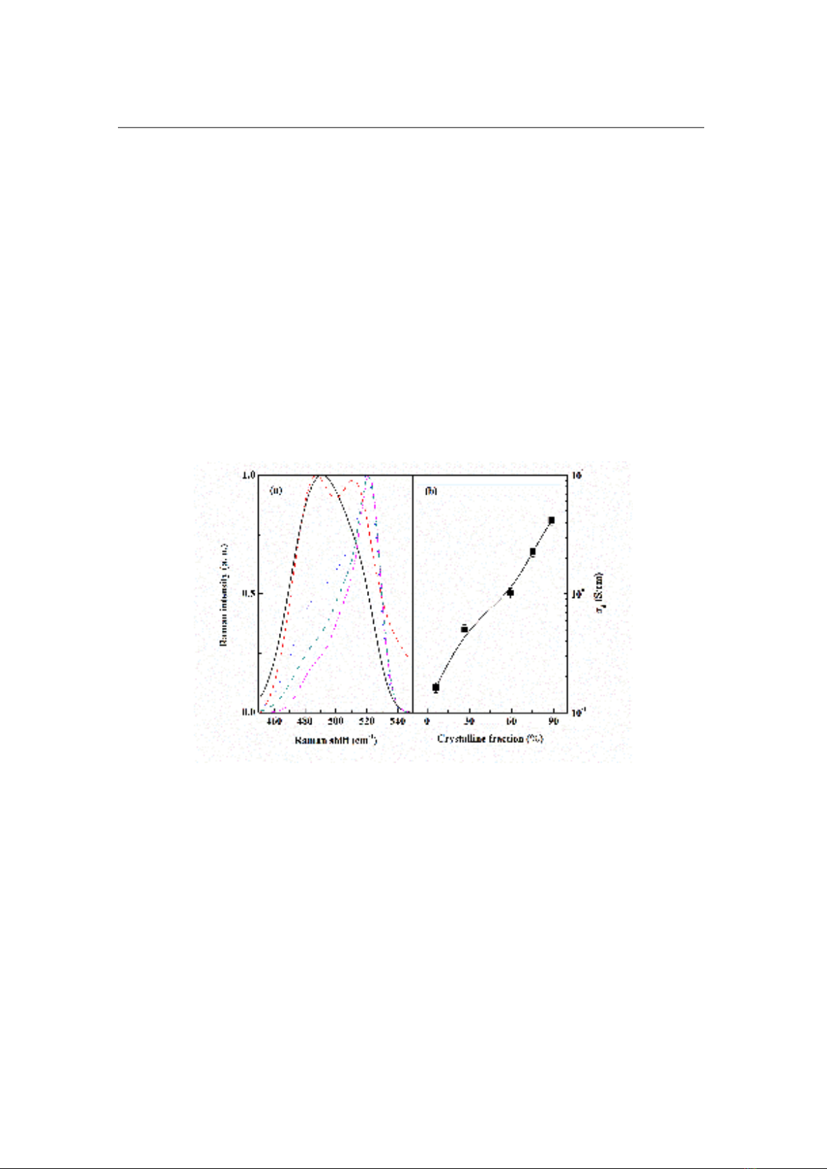
The normalized Raman spectra of the µc-Si:H(n+) layers, having a thickness in
the range 10 to 120 nm, deposited on a glass substrate are shown in Fig. 2(a). As can be
seen in Fig. 2(a), the peak intensity variation at 520 cm-1 becomes more pronounced with
increasing layer thickness. The variation in peak intensity could, hence, be related to a
higher crystalline fraction (Xc) within the films, as seen in Table 1; here, Xc was estimated
from normalized Raman spectra as described in [12]. The d respective to film
crystallinity of the µc-Si:H(n+) films was measured and shown in Fig. 2(b). It can be seen
that d increases by 26 orders of magnitude with increasing µc-Si:H(n+) crystallinity
fraction, where, the d of the c-Si:H(n+) increased from 0.16 (S/cm) to 4.16 (S/cm), with
the increases in the Xc from 6% to 89%. This result can be ascribed to the improvement
in the crystallinity fraction within the films, resulting in an evolution grain size, which,
in turn, improves carrier transportation [9].
Fig. 3 depicts the
eff of an ITO/a-Si:H(p+)/a-Si:H(i)/c-Si(n)/a-Si:H(i)/µc-
Si:H(n+)/ITO HJ structure, which the µc-Si:H(n+) properties were shown in Fig. 2. Our a-
Si:H/c-Si HJ structure showed decreasing
eff in the entire range of injection-levels of the
TẠP CHÍ KHOA HỌC VÀ CÔNG NGHỆ, Trường Đại học Khoa học, ĐH Huế
Tập 24, Số 1 (2024)
17
excess carrier density with increasing crystallinity fraction. Generally, two types of
surface passivation mechanism are suggested to be the roles: field-effect passivation,
which is indicated by excess carrier lifetime at low injection level and neutralization of
the defects of interface states, which is indicated by excess carrier lifetime at high
injection level [13]. As is well-known, at low level of carrier injection, the high film
conductivity can produce more electron concentrations within the film, resulting in
reducing Schottky-contact at the c-Si:H(n+)/ITO interface, which induced improve field-
effect passivation, as in turn, increasing
eff . It is observed that our data is in contrast to
those reported elsewhere [14], and also, contrary to our expectations, as aforementioned.
In this study,
eff shown decreased with increasing film conductivity in a low level of
injected excess carrier density. Thus, the field-effect passivation was not contributed to
the c-Si surface passivation in this investigation. Hence, only one passivation mechanism
was observed; i.e., reduction of interface defect density due to neutralization of the
defects of interface states.
Figure 2. a) Normalized Raman spectra of c-Si:H(n+) layers. Black-solid: 10 nm, red-dash: 20
nm, blue-dot: 40 nm, dark cyan-dash-dot: 70 nm, and magenta-dash-dot-dot: 120 nm. b)
Variation in room temperature dark conductivity of c-Si:H(n+) layers due to variation in the
thickness.
Film microstructure was performed to gain insight into the passivation
mechanism. The empirical spectroscopic ellipsometric data concerning the optical
constant were fitted based on the Tauc-Lorentz equation combined with the BEMA
model. The fitted results are shown in Table 1. With decreasing film crystallinity, the
values of A show a decrease, while the values of C show an increase, leading to low
density, high disorder and high hydrogen content within the films [14], where A and C
is the amplitude and the broadening parameter of the imaginary part of the dielectric


![Ảnh hưởng của chiều dày lớp Cu lên tương tác trao đổi và tính chất từ trong van spin dị hướng vuông góc [Co/Pd]: Nghiên cứu màng mỏng đa lớp](https://cdn.tailieu.vn/images/document/thumbnail/2024/20241011/vifilm/135x160/2791728643263.jpg)
![Bộ câu hỏi lý thuyết Vật lý đại cương 2 [chuẩn nhất/mới nhất]](https://cdn.tailieu.vn/images/document/thumbnail/2025/20251003/kimphuong1001/135x160/74511759476041.jpg)
![Bài giảng Vật lý đại cương Chương 4 Học viện Kỹ thuật mật mã [Chuẩn SEO]](https://cdn.tailieu.vn/images/document/thumbnail/2025/20250925/kimphuong1001/135x160/46461758790667.jpg)