Application Device Power Output Input Voltage Output Voltage Topology
Audio PKS607YN 75 W, 126 W Peak 195 - 265 VAC ±26 V, ±15 V, 5 V Flyback
DI-148 Design Idea
PeakSwitch
www.powerint.com February 2008
Multiple Output Flyback Power Supply for Audio Amplifi er
Using Magnetic Amplifi ers to Achieve Better Cross Regulation
®
Design Highlights
Effectively replaces linear transformer-based power supplies in
home audio applications
Dramatically reduces weight, allowing chassis cost reduction
Proprietary magnetic amplifi er (mag amp) approach enables
tight cross regulation of two main outputs in fl yback topology
Low component count, compact and light weight.
Energy effi ciency
>82% effi ciency at full load
<800 mW no-load power consumption at 265 VAC
Reduces heat sink requirements and eliminates need for
separate standby supply
Excellent transient response – improves audio quality
Integrated frequency jittering, together with a simple EMI fi lter,
allows for CISPR-22/EN55022B conducted EMI compliance
(see Figure 2)
Integrated safety/reliability features:
Accurate, auto-recovering, hysteretic thermal shutdown func-
tion maintains safe PCB temperatures under all conditions
Latching shutdown protects against output short circuits and
open feedback loops
•
•
•
•
•
•
•
•
•
•
•
•
•
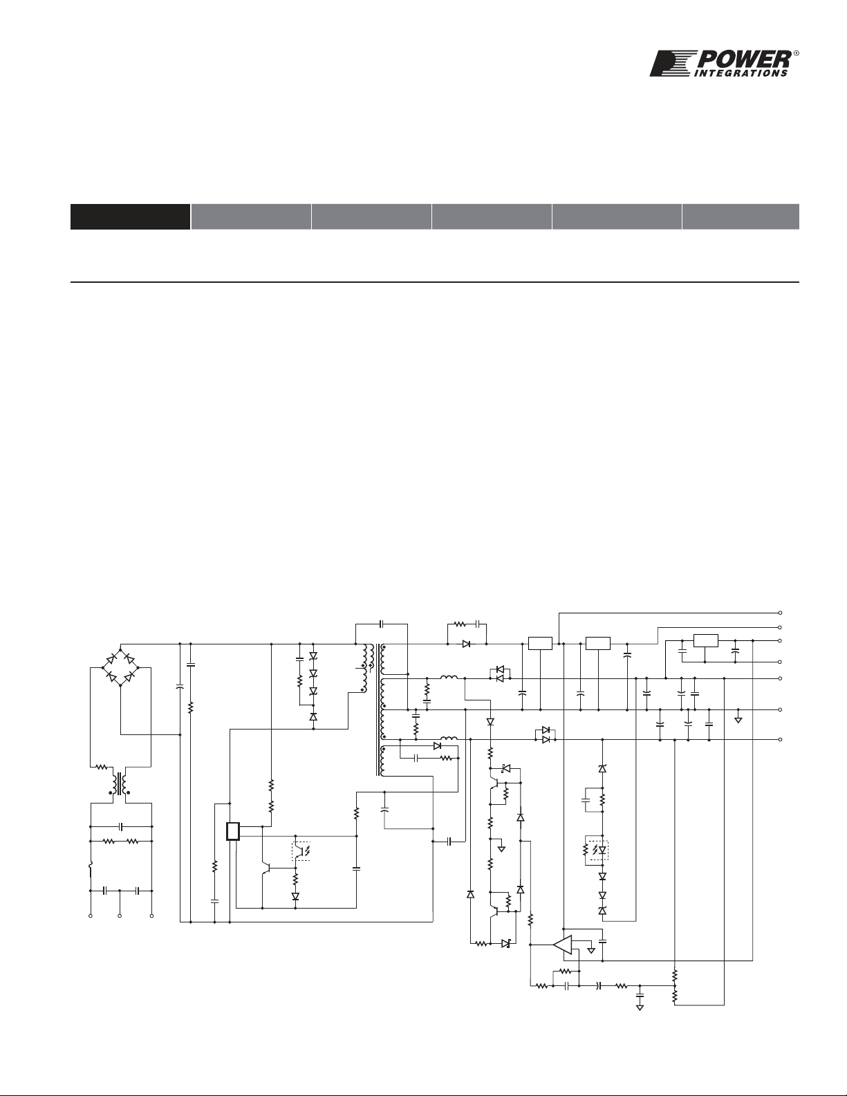
Figure 1. Schematic of a 75 W Continuous and 126 W Peak Audio Amplifi er Power Supply.
Operation
The universal input power supply shown in Figure 1 has multiple
outputs, ±26 VDC, ±15 VDC, and +5 VDC. The ±26 V outputs
can each deliver a minimum output current of 2.42 A peak (ther-
mally limited) and 1.45 A continuous. Additionally, the voltage
regulation and, importantly, transient response is excellent over the
entire load range (no-load to full load).
The controller in U1 skips switching cycles to regulate the output
voltage, based on feedback to its EN/UV pin. When the current
pulled out of this pin exceeds 240 µA, a low logic level (disable) is
generated. At the beginning of each cycle, the EN/UV pin state is
sampled, and if high, the power MOSFET is turned on for that
cycle (enabled); otherwise the power MOSFET remains off
(disabled). During start-up, switching is inhibited until the input
voltage is above the under-voltage threshold, determined when a
current >25 µA fl ows into the EN/UV pin.
D6
D3 1N4148
UF4002
C5
47 uF
C48
33 pF
1 kV
35 V
R16
68 1/2 W
C23
C26
100 F
25 V
C19
100 F
25 V
C49
470 pF
100 V
C27
47 F
10 V
C20
680 nF
50 V C28
100 F
25 V
C16
680 nF
50 V
C15
680 nF
50 V
C11
330 F
50 V
C10
330 F
50 V
R21
130 U2A
PC817D
C46
47 F
10 V
C37
10 nF
50 V
C35
220 nF
50 V
U7A
LM358P
C39
1 nF
50 V
R30
49.9 k1%
R50
10 R32
1 kR27
1 kR45
2.7 kR46
5.1 k1/8 W
R23
510 R24
510 R48
5.1 k1/8 W
R47
2.7 kR52
68 k1/2 W
R53
68 k1/2 W
R31
49.9 k1%
R43
1 kD19
1N4148
D21
1N4148
D20
SB160
D5
BYV32-
200
D9
BYV32-
200
D13
BAV20
D18
SB160
D12
BAV20
D11
1N4148
D10
1N4148
VR5
1N5254B
27 V
C34
100 nF
50 V
VR4
1N5253B
25V
C13
330 F
50 V
C14
330 F
50 V
330 pF
N.C.
T1
EER28
4
8,9
5
7
1
2,3
6
12
C47
1 nF
50 V
R5
2M
VR1
P6KE91A
R3
4.7 kR4
2M
D2
UF4005
C4
330 nF
R6
1501/2 W
C6
470 pF
1kV
C8
2.2 nF
250 VAC
U2B
PC817D
C7
4700pF
1kV
R49
10 1/2 W
R51
100 1/2 W
R7
2.2 C9
2.2 nF
250 VAC
VR2
R1
1.3 MC17
220 pF
250 VAC
C45
100
F
400 V
C1
275 VAC
330 nF
R2
1.3 M
D7-8,D16-17
1N4007
D22
1N4148
F1
C18
220 pF
250 VAC
L1
10 mH
3.15 A
NPEL
tO
P6KE91A
U1
PKS607YN
PeakSwitch
RT1
VR3
P6KE91A
10
11
3
2
L2
MP1305
PI-4884-021108
15 V, 150 mA
5 V, 150 mA
26 V, 1.45 A
195 - 265
VAC
-26 V, 1.45 A
RTN
RTN
-15 V, 150 mA
R44
100 kR26
2 kQ2
MPSA42
Q3
2N3904
U8
LM7915
U5
LM78L05
U6
UA7815
IN OUT
GND
IN OUT
GND
IN OUT
GND
Q1
2N5401
D
S
EN/UV
BP
GND
L3
MP1305
C50
470 pF
100 V

Power Integrations
5245 Hellyer Avenue
San Jose, CA 95138, USA.
Main: +1 408-414-9200
Customer Service
Phone: +1-408-414-9665
Fax: +1-408-414-9765
Email: usasales@powerint.com
On the Web
www.powerint.com
A
02/08
Power Integrations reserves the right to make changes to its products at any time to improve reliability or manufacturability. Power
Integrations does not assume any liability arising from the use of any device or circuit described herein. POWER INTEGRATIONS
MAKES NO WARRANTY HEREIN AND SPECIFICALLY DISCLAIMS ALL WARRANTIES INCLUDING, WITHOUT LIMITATION, THE IMPLIED
WARRANTIES OF MERCHANTABILITY, FITNESS FOR A PARTICULAR PURPOSE, AND NON-INFRINGEMENT OF THIRD PARTY RIGHTS.
The products and applications illustrated herein (transformer construction and circuits external to the products) may be covered by
one or more U.S. and foreign patents or potentially by pending U.S. and foreign patent applications assigned to Power Integrations.
A complete list of Power Integrations' patents may be found at www.powerint.com. Power Integrations grants
its customers a license under certain patent rights as set forth at http://www.powerint.com/ip.htm.
The PI logo, TOPSwitch, TinySwitch, LinkSwitch, DPA-Switch, PeakSwitch, EcoSmart, Clampless, E-Shield, Filterfuse, StackFET,
PI Expert and PI FACTS are trademarks of Power Integrations, Inc. Other trademarks are property of their respective companies.
©2007, Power Integrations, Inc.
DI-148
The primary feedback circuit is closed across the ±26 V (52 V)
outputs via VR4, U2A and VR5. This ensures that the sum of
voltages across the ±26 V outputs is regulated. For improved
cross-regulation, two separate magnetic amplifi ers (mag amps)
are used on the ±26 V outputs. A mag amp is a saturable reactor
or inductor that uses a core material that has a rectangular B-H
curve. Adjusting the current (magnetic fl ux) in the mag amp
adjusts the period that it blocks current fl ow.
Here two magnetic amplifi ers (L2 and L3) are used for improved
cross regulation. This is especially relevant for audio designs as
power is drawn from the supply at audio frequencies. The highest
output power component occurs at lower frequency where current
is alternately drawn from each output but not simultaneously.
By adjusting the current in L2 and L3, the circuitry formed by U7A,
Q1 and Q2 determines the proportion of the energy stored in the
transformer that is delivered to the +26 V and -26 V outputs
during the off time of the PeakSwitch internal MOSFET. At the
extreme, with one output fully loaded and the other at no-load,
almost all the energy is delivered to the output under full load.
Importantly, both outputs cannot be simultaneously blocked,
which would cause excessive clamp dissipation. Even with very
large load transients 25%-100% that are common in audio
supplies, the output regulation is maintained within ±5% on both
outputs.
Common mode choke, L1, and the two Y-capacitors, C8 and C9,
form the common mode EMI fi lter. Common mode choke L1 also
works in conjunction with X-capacitor C1 to provide differential
mode EMI fi ltering.
Key Design Points
The high crest factor of the music source allows physically
smaller heatsinks.
The auxiliary ±15 VDC and +5 VDC outputs are obtained from
a linear regulator. To limit the power dissipation in the (5 V and
15 V) linear regulators, a second 18 V output was added to
transformer T1.
As the value of X capacitor C1 is above 0.1 μF, safety agency
requirements specify that it R1 and R2 should be used to
discharge C1. Resistors R1 and R2 are chosen such that
(R1 + R2) × C1 ≤ 1 s.
To reduce grouping of switched cycles, a high gain optocoupler,
U2, was used to drive small signal transistor Q3, which pulls
current out of the EN/UV pin. Capacitor C34 adds high
frequency gain to the feedback signal.
In a three wire system, placing Y capacitors (C17, C18) between
line/neutral and earth helps reduce common mode EMI.
•
•
•
•
•
Transformer Parameters
Core Material EER28 NC-2H or equivalent,
gapped for ALG of 139 nH/t²
Bobbin EER28, 12 pin, Vertical
Winding Details
Add 3 mm margins on both sides of bobbin
Primary: 16T × 2, AWG30, tape
Shield: 1T × 1, foil 2 mils thick, 3 layers tape
+26 V: 8T × 2, AWG23, 1 layer tape
-26 V: 8T × 2, AWG23, 1 layer tape
18 V: 6T × 2, AWG28, tape
Bias: 5T × 2, AWG30, tape
Primary: 17 T × 2, AWG30, 2 layers tape
Winding Order Primary (4–2), Shield (NC–1), +26 V (7–8), -26 V
(9-11), 18 V (12-10), Bias (5-6), Primary (2-1)
Primary Inductance 151 μH, ±20%
Primary Resonant
Frequency 2 MHz (minimum)
Leakage
Inductance 5 μH (maximum)
Table 1. Transformer Parameters.
(NC = No Connection, TIW = Triple Insulated Wire)
Figure 2. Conducted EMI at 230 VAC With Output Grounded (Worst Case).
PI-4885-110707
1.0 0.15 10.0 100.0
-20
-10
0
10
20
30
40
50
60
80
70
MHz
dB
µ
V
QP
AV
The core size and the winding wire diameter sizes (see Table 1)
were chosen based on the average of the peak and the
continuous output power.
An RC snubber (R51and C48) was added between drain and
source of U1 to reduce radiated EMI.
•
•


%20--%3e%3cdefs%3e%3cstyle%3e%20.st0%20{%20fill:%20%23fff;%20}%20.st1%20{%20fill:%20%237800fa;%20}%20%3c/style%3e%3c/defs%3e%3cpath%20class='st1'%20d='M117.78,12.18H43.11c2.9,3.47,4.65,7.94,4.65,12.82,0,5.6-2.3,10.66-6.01,14.29h76.02l7.22-13.56-7.22-13.56Z'/%3e%3cg%3e%3cpath%20class='st0'%20d='M53.58,26.17h-.59v-1.46h.59v-4.96h2.83c1.78,0,2.67.94,2.67,2.82v5.76c0,1.87-.89,2.81-2.67,2.81h-2.83v-4.96ZM55.36,21.37v3.34h1.1v1.46h-1.1v3.34h1.01c.61,0,.91-.37.91-1.1v-5.93c0-.74-.3-1.1-.91-1.1h-1.01Z'/%3e%3cpath%20class='st0'%20d='M65.99,31.14h-1.8l-.31-2.07h-2.19l-.31,2.07h-1.64l1.82-11.39h2.62l1.82,11.39ZM65.28,18.04c-.25.46-.51.77-.75.94-.21.15-.47.22-.79.22-.26,0-.57-.07-.92-.22l-.38-.15c-.14-.05-.26-.07-.37-.07-.3,0-.53.18-.71.54l-.91-.68c.25-.46.51-.77.75-.94.21-.14.48-.21.79-.21.26,0,.57.07.92.21l.38.15c.14.05.26.07.37.07.3,0,.53-.18.71-.54l.91.68ZM61.91,27.52h1.73l-.87-5.76-.87,5.76Z'/%3e%3cpath%20class='st0'%20d='M74.53,26.89v1.52c0,1.91-.89,2.86-2.67,2.86s-2.67-.95-2.67-2.86v-5.93c0-1.91.89-2.86,2.67-2.86s2.67.95,2.67,2.86v1.11h-1.69v-1.22c0-.75-.31-1.12-.93-1.12s-.93.37-.93,1.12v6.15c0,.74.31,1.11.93,1.11s.93-.37.93-1.11v-1.63h1.69Z'/%3e%3cpath%20class='st0'%20d='M81.4,31.14h-1.8l-.31-2.07h-2.19l-.31,2.07h-1.64l1.82-11.39h2.62l1.82,11.39ZM75.9,19.2l1.52-1.91h1.71l1.51,1.91h-1.61l-.76-.95-.75.95h-1.61ZM77.32,27.52h1.73l-.87-5.76-.87,5.76ZM83.1,15.99l-1.76,1.91h-1.26l1.17-1.91h1.86Z'/%3e%3cpath%20class='st0'%20d='M84.86,19.75c1.78,0,2.67.94,2.67,2.82v1.48c0,1.87-.89,2.81-2.67,2.81h-.85v4.28h-1.79v-11.39h2.64ZM84.01,21.37v3.86h.85c.58,0,.87-.36.87-1.08v-1.71c0-.71-.29-1.07-.87-1.07h-.85Z'/%3e%3cpath%20class='st0'%20d='M93.51,19.75c1.78,0,2.67.94,2.67,2.82v1.48c0,1.87-.89,2.81-2.67,2.81h-.85v4.28h-1.79v-11.39h2.64ZM92.66,21.37v3.86h.85c.58,0,.87-.36.87-1.08v-1.71c0-.71-.29-1.07-.87-1.07h-.85Z'/%3e%3cpath%20class='st0'%20d='M98.8,31.14h-1.79v-11.39h1.79v4.88h2.03v-4.88h1.83v11.39h-1.83v-4.88h-2.03v4.88Z'/%3e%3cpath%20class='st0'%20d='M105.36,24.55h2.46v1.62h-2.46v3.34h3.09v1.63h-4.88v-11.39h4.88v1.63h-3.09v3.18ZM108.17,17.29l-1.76,1.91h-1.26l1.17-1.91h1.86Z'/%3e%3cpath%20class='st0'%20d='M112.2,19.75c1.78,0,2.67.94,2.67,2.82v1.48c0,1.87-.89,2.81-2.67,2.81h-.85v4.28h-1.79v-11.39h2.64ZM111.35,21.37v3.86h.85c.58,0,.87-.36.87-1.08v-1.71c0-.71-.29-1.07-.87-1.07h-.85Z'/%3e%3c/g%3e%3ccircle%20class='st1'%20cx='25'%20cy='25'%20r='20'/%3e%3cpath%20class='st0'%20d='M32.78,19.27c2.92,0,4.43,2.55,5.28,5.33l.71,2.17c.14.38-.33.75-.71.75h-5.61c.19-.33.24-.71.09-1.08l-.75-2.45c-.43-1.32-.99-2.64-1.79-3.77.75-.57,1.65-.94,2.78-.94h0ZM25,18.38c3.25,0,4.9,2.78,5.89,5.89l.76,2.45c.14.42-.33.8-.8.8h-11.69c-.42,0-.94-.38-.8-.8l.75-2.45c.99-3.11,2.64-5.89,5.89-5.89h0ZM25,11.35c1.74,0,3.11,1.37,3.11,3.11s-1.37,3.11-3.11,3.11-3.11-1.41-3.11-3.11,1.41-3.11,3.11-3.11h0ZM17.27,19.27c1.08,0,1.98.38,2.73.94-.8,1.13-1.37,2.45-1.74,3.77l-.8,2.45c-.14.38-.05.75.09,1.08h-5.56c-.42,0-.9-.38-.75-.75l.71-2.17c.9-2.78,2.41-5.33,5.33-5.33h0ZM17.27,12.91c1.51,0,2.78,1.27,2.78,2.83s-1.27,2.83-2.78,2.83-2.83-1.27-2.83-2.83,1.27-2.83,2.83-2.83h0ZM32.78,12.91c1.56,0,2.78,1.27,2.78,2.83s-1.23,2.83-2.78,2.83-2.83-1.27-2.83-2.83,1.27-2.83,2.83-2.83h0ZM27.07,28.56v.09c0,.57-.24,1.08-.61,1.46h0v.05c-.38.33-.9.57-1.46.57s-1.08-.24-1.46-.61h0c-.38-.38-.61-.9-.61-1.46v-.09h1.41v.09c0,.19.05.38.19.47v.05c.09.09.28.19.47.19s.38-.09.47-.19v-.05c.14-.09.24-.28.24-.47t-.05-.09h1.41ZM30.99,28.56v.09c0,1.65-.66,3.16-1.74,4.24-1.08,1.08-2.59,1.79-4.24,1.79s-3.16-.71-4.24-1.79l-.05-.05c-1.04-1.08-1.7-2.55-1.7-4.2v-.09h1.41v.09c0,1.27.47,2.4,1.27,3.25h.05c.85.85,1.98,1.37,3.25,1.37s2.4-.52,3.25-1.37c.85-.8,1.37-1.98,1.37-3.25v-.09h1.37ZM34.99,28.56v.09c0,2.78-1.13,5.28-2.92,7.07-1.79,1.79-4.29,2.92-7.07,2.92s-5.23-1.13-7.07-2.92c-1.79-1.79-2.92-4.29-2.92-7.07v-.09h1.41v.09c0,2.4.94,4.53,2.5,6.08,1.56,1.56,3.72,2.5,6.08,2.5s4.52-.94,6.08-2.5c1.56-1.56,2.5-3.68,2.5-6.08v-.09h1.41Z'/%3e%3c/svg%3e)