
TNU Journal of Science and Technology
229(06): 41 - 50
http://jst.tnu.edu.vn 41 Email: jst@tnu.edu.vn
FINE-GRAIN CLOCK GATING TECHNIQUE FOR A POWER SAVING 32-BIT
PIPELINED MULTIPLIER IN ACTIVE MODE
Vo Minh Huan*, Pham Van Khoa
Ho Chi Minh University of Technology and Education
ARTICLE INFO
ABSTRACT
Received:
30/11/2023
Regularly, the clock gating enable signal is generated based on coarse grain
clock gating where the clock enable signal is generated from system view.
This study proposes the fine grain clock gating where the clock enable signal
is generated from block view. The clock enable signal is self-generated based
on look ahead technique which is applied to 32-bit pipelined multiplier. A
pipelined multiplier breaks multiplication process into multiple stages, where
each stage performs a small part of overall multiplication. The clock gating
enable signal is self-generated from each pipeline stage which can be looked
ahead to gate clocks to flipflops. The proposed 32-bit look ahead clock gating
(LACG) pipelined multiplier using fine-grain technique shows the ability to
efficiently save power consumption compared to the normal 32-bit pipelined
multiplier using coarse grain technique. The study proves results on 32-bit
pipelined adder and 32-bit pipelined multiplier in terms of power
consumption, utilization area and functionality. The testbench is performed
by five different testcases. The simulation results show the proposed
multiplier saves power consumption up to 13.2% in case of random input test
case compared to the normal multiplier. However, the proposed multiplier
still has more utilization area overhead than the normal pipelined multiplier.
Revised:
22/3/2024
Published:
22/3/2024
KEYWORDS
Coarse grain
Fine grain
Look ahead clock gating
Multiplier
Pipelined technique
KỸ THUẬT CLOCK GATING CHỈNH TINH CHO MẠCH NHÂN ĐƯỜNG ỐNG
32 BIT TIẾT KIỆM CÔNG SUẤT TRONG CHẾ ĐỘ TÍCH CỰC
Võ Minh Huân*, Phạm Văn Khoa
Trường Đại học Sư phạm Kỹ thuật Thành phố Hồ Chí Minh
THÔNG TIN BÀI BÁO
TÓM TẮT
Ngày nhận bài:
30/11/2023
Thông thường, tín hiệu cho phép clock gating được tạo dựa trên clock gating
chỉnh thô ở đó tín hiệu cho phép clock được tạo tại mức hệ thống. Nghiên cứu
này đề xuất clock gating chỉnh tinh ở đó tín hiệu cho phép clock gating được
tạo ra tại mức khối. Tín hiệu cho phép clock gating được tự tạo dựa trên kỹ
thuật nhìn trước về khả năng clock gint được áp dụng cho mạch nhân đường
ống 32 bit. Mạch nhân theo đường ống chia quá trình nhân thành nhiều giai
đoạn, trong đó mỗi giai đoạn thực hiện một phần nhỏ của mạch nhân. Tín
hiệu cho phép clock gating được tự tạo từ mỗi giai đoạn đường ống, tín hiệu
này có thể được nhìn thấy trước để tắt clock đến flipflop. Mạch nhân đường
ống nhìn thấy trước clock gating (LACG) 32 bit dùng kỹ thuật chỉnh tinh
được đề xuất cho thấy khả năng tiết kiệm điện năng tiêu thụ một cách hiệu
quả so với mạch nhân theo đường ống 32 bit thông thường dùng kỹ thuật
chỉnh thô. Nghiên cứu chứng minh kết quả trên bộ cộng đường ống 32 bit và
mạch nhân đường ống 32 bit về mức tiêu thụ điện năng, diện tích sử dụng và
chức năng. Testbench được thực hiện bởi năm trường hợp kiểm tra khác nhau.
Kết quả mô phỏng cho thấy mạch nhân được đề xuất tiết kiệm điện năng tiêu
thụ lên tới 13,2% trong trường hợp thử nghiệm ngõ vào ngẫu nhiên so với
mạch nhân thông thường. Tuy nhiên, mạch nhân được đề xuất vẫn có nhiều
chi phí diện tích sử dụng hơn mạch nhân theo đường ống thông thường.
Ngày hoàn thiện:
22/3/2024
Ngày đăng:
22/3/2024
TỪ KHÓA
Chỉnh thô
Chỉnh tinh
Clock gating nhìn thấy trước
Bộ nhân
Kỹ thuật đường ống
DOI: https://doi.org/10.34238/tnu-jst.9321
* Corresponding author. Email: huanvm@hcmute.edu.vn

TNU Journal of Science and Technology
229(06): 41 - 50
http://jst.tnu.edu.vn 42 Email: jst@tnu.edu.vn
1. Introduction
In a digital system, data is represented in binary form and processed using digital circuits. The
ALU is a center component of these circuits that is responsible for performing basis arithmetic
operations such as addition, subtraction, multiplication, and division as well as logical operations
such as AND, OR, NOT, and XOR. The high-speed digital system consists of digital signal
processing algorithms such as FFT and FIR which the multiplier is main arithmetic logic. In
detail, 8.72% of all instructions are multiplier in a typical scientific program [1]. The multiplier is
a fundamental arithmetic component that is responsible for performing arithmetic, and logic
operations on binary data. The multiplier decides ALU performance. The role of multiplier in the
ALU is to perform multiplication operations on binary data. Multiplication is required in many
computer applications including graphics processing, scientific calculations, and cryptography.
By implementing a multiplier in the ALU, the CPU can perform multiplication quickly and
efficiently [2].
A normal multiplier also known as a single cycle multiplier, performs the entire multiplication
operation in a single clock cycle [3]. It means that the input operands are multiplied in a single
stage and results are immediately available at the output. While this approach is simple and
straightforward, it can be relatively slow and resource-intensive for large operands. On the other
hand, a pipelined multiplier breaks multiplication process into multiple stages, where each stage
performs a small part of overall multiplication [4], [5]. The input operands are split into smaller
pieces which are processed in parallel. The results of each stage are then added together to
produce the final product. The advantage of a pipelined multiplier is that it can perform
multiplication operations much faster than a normal multiplier. This is because the pipelined
architecture allows for parallel processing of the operands, reducing the overall processing time
required. Thus, a pipelined multiplier is often used in high-speed applications such as in digital
signal processing, graphics processing, and cryptography to perform multiplication operations
quickly and efficiently [4].
Pipeline technique is applied to different fields [5] – [8]. In general, a pipeline technique
involves breaking down a complex task or process into a series of smaller, more manageable
steps or stages, with data flowing from one stage to another by breaking down a complex task
into smaller stages, each with a specific purpose. The pipeline technique allows for
parallelization and efficient resource utilization. Different stages of the pipeline can be executed
concurrently, reducing overall processing time and increasing throughput. By applying the
pipeline technique to the multiplier design, the multiplication operation can be divided into
several stages, allowing for parallelism and improved efficiency. By breaking down the
multiplication process into these stages, each stage can be implemented as a separate pipeline
stage with its own set of circuitries. This enables parallel execution of multiple multiplications
and improves the overall throughput and performance of the multiplier. The pipeline stages can
be overlapped so that while one multiplication is in progress, the subsequent multiplication can
begin in the following stages, minimizing idle time and maximizing utilization [4], [9].
Clock gating, a widely employed method in numerous low-power circuits, serves the purpose
of curtailing dynamic power dissipation [10], [11]. Its fundamental principle revolves around
interrupting the clock signal when the circuit remains inactive. The crux of the clock gating
technique lies in deactivating the clock signal to prevent unnecessary signal propagation through
the circuit during periods of inactivity or standby mode. This measure is taken to avert inefficient
power consumption stemming from needless signal switching when not required. The approach
encompasses diverse clock gating methodologies like Synthesis Based Clock Gating, latch data-
driven clock gating, and Auto-Gated Flip-Flops, each applied across a spectrum of applications
including counters, digital clock circuits, linear feedback shift registers, and others [10] – [15].

TNU Journal of Science and Technology
229(06): 41 - 50
http://jst.tnu.edu.vn 43 Email: jst@tnu.edu.vn
Clock gating is a prevalent technique predominantly applied at the architectural design level,
managing the activation and deactivation of the clock for the entire System-on-Chip (SoC). Its
primary purpose is to conserve power by initiating sleep mode or waiting for external system
requests [10], [11]. At the block level, clock gating governs the activation or deactivation of
specific blocks within the system, allowing them to transition between idle and active states.
However, when the clock signal is distributed across multiple sub-clock domains with differing
frequencies or distinct operational principles within a block, the efficacy of implementing clock
gating diminishes at the block level. This occurs because not all functional subblocks within a
block enter idle or active states simultaneously. Therefore, the optimal power-saving potential of
clock gating is realized only when the entire block transitions to sleep or idle mode. At certain
instances, specific functional subblocks might remain active to maintain the system's necessary
state, rendering traditional clock gating ineffective.
To refine power conservation by exerting control over clock gating at a finer granularity, each
subblock should possess its clock control. This would enable individual subblocks to be
independently clocked and self-selected based on control signals, allowing for precise
adjustments to power consumption levels. The study applies this proposed concept to the
pipelined system to build a lower power multiplier using fine-tuning clock gating technique each
subblock. The study uses look ahead clock gating technique to calculates the clock self-enable
signals of each FF before each cycle, based on the current cycle data of those FFs on which it
depends. The content of the study is not simply using the usual clock gating technique. The
author focuses on proposing a fine-grain clock gating method, used to optimize the power
consumption on the clock network. Conventional clock gating technique only applies to a large
system such as a SoC system. If the system is idle, the clock signal will be gated so as not to
increase the switching of the clock network. The fine grain clock gating technique proposed in
this paper focuses on reducing switching performance in small blocks (subblocks) rather than in a
large system that is called a coarse grain clock gating technique. Given that, in a large active SoC
block, there are bound to be a few subblocks that are not functional but still consume clock
signals to switch, these blocks should be clocked off to reduce switching on clock network in
active mode.
This study applies this fine grain clock gating technique based on look ahead clock gating
technique to the 32-bit pipelined multiplier. It is possible to combine clock gating and multiplier
circuits to create more power efficient designs. The next section presents the methods to propose
fine grain clock gating technique and designs the look ahead clock gating technique to the 32-bit
Pipelined multiplier. The simulation result is presented in Section 3. Finally, the study presents
the conclusion.
2. Material and methods
2.1. Fine grained clock gating technique
Figure 1a illustrates the conventional clock gating technique. In this setup, a global clock
signal (GCLK) undergoes multiplication with the enable signal EN via an AND gate, governing
the functionality of logic subblocks 1, 2, and 3. When the EN signal equals 0, the AND gate
output becomes logic 0, leading to the deactivation of the GCLK clock. Consequently, the
network clock is deactivated, depriving the logic blocks of operational pulses. Conversely, when
the EN signal equals 1, the logic blocks synchronize their operations with the GCLK signal,
enabling the execution of switching functions within the logic circuit.
During normal operation in active mode, it's common for logic subblocks (subblocks 1, 2, and
3) not to be simultaneously active to fulfill their functions. For instance, if logic subblock 1
remains inactive while subblocks 2 and 3 continue to operate, serving the system's functions, it
becomes advantageous to implement clock gating specifically at logic block 1 to conserve the
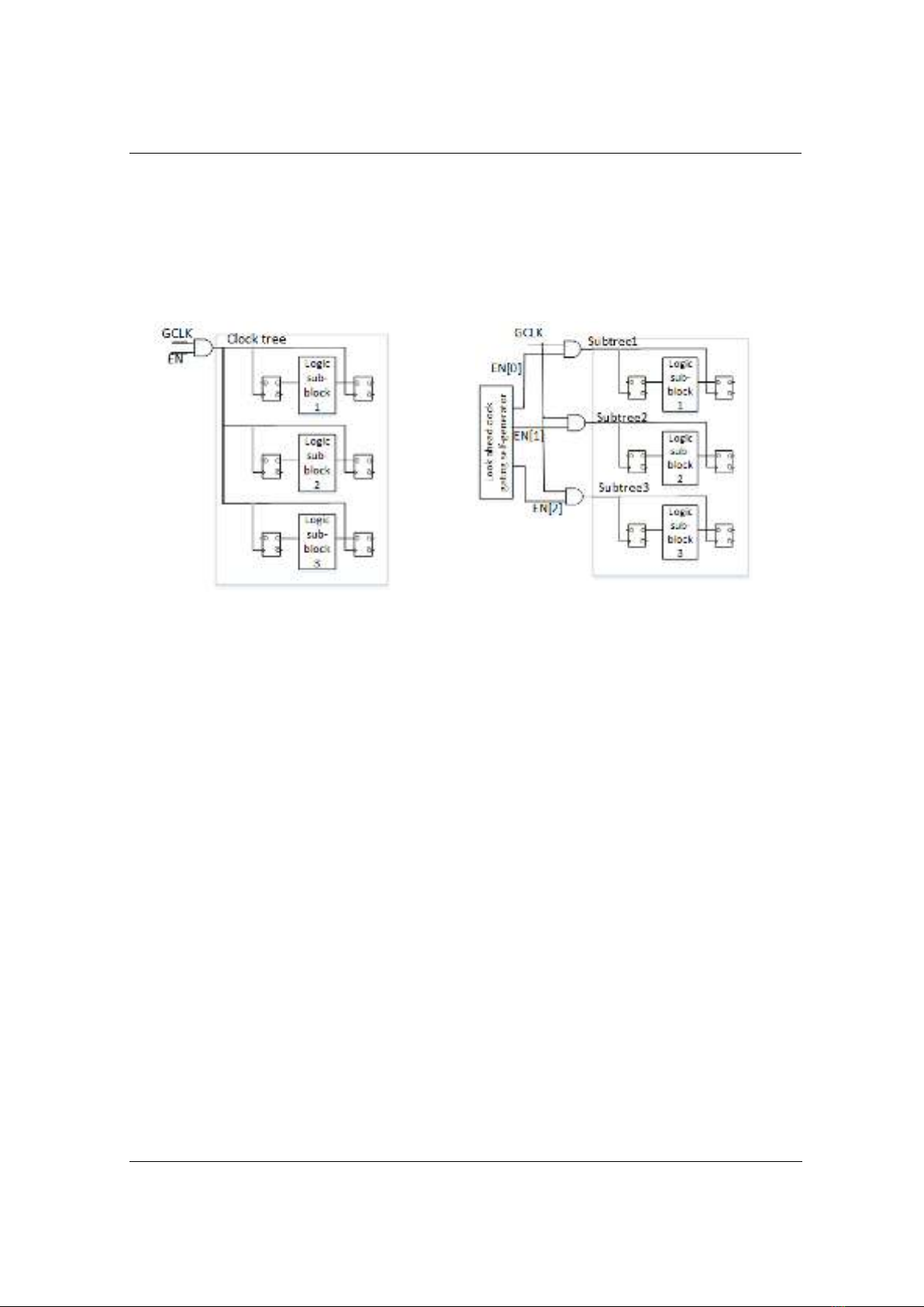
TNU Journal of Science and Technology
229(06): 41 - 50
http://jst.tnu.edu.vn 44 Email: jst@tnu.edu.vn
system's switching power, as demonstrated in Figure 1b. In this setup, a lookahead clock gating
self-generator block generates three distinct enable signals (EN[0], EN[1], and EN[2]) based on
the current operational status of the system. These signals, along with the GCLK signal, serve as
inputs to AND gates (as depicted in Figure 1b). The resulting output from these AND gates
controls the activation and deactivation of the GCLK pulse for the three-block logic circuit. By
dynamically enabling or disabling logic subblocks 1, 2, and 3 in response to the system's working
status, even while the circuit is operational, a substantial amount of wasted switching energy
within the system can be effectively conserved.
(a)
(b)
Figure 1. (a) Block diagram of normal coarse grain clock gating technique
b) block diagram of the proposed fine grain clock gating technique [16]
When assessing the architectural area cost between two distinct clock gating methodologies,
it's evident that the fine-grain clock gating approach involves supplementary hardware
components. This includes the incorporation of a lookahead clock gating signal generator block
along with a clock gating implementation block comprising AND gates. This highlights that the
fine-grain clock gating module necessitates extra hardware resources to enable the segregation of
the EN control signal and the subsequent implementation of the fine-grain clock gating
architecture using AND gates.
Typically, clock gating involves utilizing the enable signal in conjunction with the clock
signal through an AND gate, depicted in both Figures 1a and 1b. Figure 1a showcases the
standard clock gating technique utilizing a single main clock (GCLK) to generate the clock tree
signal steering the flip-flops. When employing this method (Figure 1a), a low EN signal results in
bringing the clock tree signal to a non-switching low level. Consequently, the flip-flop data lines
governed by the clock tree remain inactive. Consider the scenario in Figure 1a, where the clock
tree signal operates normally, yet subblock1 logic transitions to an idle state. In this setup, to
deactivate the clock tree, the system must wait for both subblock 2 and subblock 3 logics to
become idle, causing unnecessary switching power wastage in subblock 1. Conversely, in Figure
1b, the global clock tree (GCLK) domain is partitioned into subtree domains (subtree1, subtree2,
and subtree3) for their respective flip-flop data lines. Each subtree is associated with an enable
signal fine-tuning the switching activation of its data lines. Consequently, while some subtree
clock domains, like subtree2 and subtree3, may be active, allowing transitions, other subtree
clock domains, e.g., subtree1, remain idle without switching. Therefore, subtree1 deactivates,
preserving energy, while subtree2 and subtree3 continue normal operation, along with the main
clock domain (GCLK) maintaining its regular function.

TNU Journal of Science and Technology
229(06): 41 - 50
http://jst.tnu.edu.vn 45 Email: jst@tnu.edu.vn
2.2. LACG technique
The comparison between input D and output Q is performed by an XOR gate. The output of
XOR gate is fed to the AND gate to generate the required clock signal (CLK_G) for the flipflop.
When both D and Q states are the same, the clock signal will remain low, and no power is
consumed to switch. When their states are different, the clock signal will be the original clock
signal and can make the necessary transitions to change the flip flop's state. The same technique
can be used for falling edge flipflops using an XNOR or an OR gate as shown in Figure 2 (a).
The fine grain clock gating technique can gate clock signal and turn off the clock signal
according to the Look Ahead Clock Gating method. The clock enable signal generator uses an
XOR gate and an AND gate to self-generate the gating clock signal. The clock enable signal self-
generator performs a preview of the signal changes at adjacent times to gating the signals into the
FFD subblock in the circuit. The Q output of the FFD under consideration will be XORed with
the D input (Q_(n-1)) of the preceding FFD. The output of the XOR will be AND with CLK. If
there is no data change, CLK will be turned off and vice versa. Because of gating each FFD, the
AND gate is used as the gating logic.
Figure 2(b) shows an 8-bit adder. A 32-bit adder using the pipeline method is designed from
this 8-bit adder. Four 8-bit adders are combined to create a 32-bit adder. The 8-bit full adder has a
design based on the carry ripple adder which is presented with input A [7:0] and B [7:0], carry
input Cin and carry output Cout, Summation output S [0:7]. The summation of the most
significant bits is only available after the carry signal has rippled through the adder from the least
significant stage to the most significant stage. In Figure 2(b), an 8-bit LACG register shifts the
input data including 8 LACG D-flipflops. The clock signal is applied flip flop D to control it as
data is changed. The proposed idea is to build an adder using the clock signal that implements an
adder with the look ahead clock gating method. The clock is used to control the data translation
into the FFDs. If there is no change in the input signal, the clock will be turned off, the input
signal and the carry bit will not be shifted. Conversely, when there is a change in input data, the
FFD can gating the input data and allowing the carry bit to shift. The last carry bit (the 7th bit) of
the previous Full Adder is shifted to the next Full Adder to generate a concatenated signal that
works continuously.
2.3. The proposed multiplier
After designing the 8-bit Full Adder, we concatenate four 8-bit adders together to create a 32-
bit adder as shown in Figure 3(a). The additional flip flops are designed to create a full 32-bit
pipelined Adder. The flip flops have the function of buffering data, creating synchronization at
the adder's output, and will shift as soon as the output response is detected. Thus, these flipflops
separate from other adders so that they can function continuously without interruption. At the
same time, these flip flops are also specially designed according to LACG technique gating the
clock signals to reduce the power of this adder.
The next result will be reached after each clock pulse. The result of the summation of two
numbers A [31:0] and B [31:0] is output S [31:0]. Therefore, the operation execution time will be
significantly reduced compared to the adder circuit without a pipeline design. The results of the
without pipelined multiplier operations must wait a time equal to the response time of the first
result while the resources in the circuit are only maintained not used.
Figure 3 (b) shows block diagram of 32-bit LACG Pipelined Multiplier. The proposed
multiplier consists of two inputs that B [31:0] inputs are multiplied by A [31:0] inputs. The logic
result is synthesized from the AND gate set. The logic result at the AND gate is fed into the 32-
bit pipelined adders. The resulting cascades of the previous adder are then fed into the next adder
following the multiplication of the succeeding stages up to the end of the 31st bit. In addition, the
first A0 bits and the S0 bits of the previous stages will be buffered to output in a synchronous


![Bài tập tối ưu trong gia công cắt gọt [kèm lời giải chi tiết]](https://cdn.tailieu.vn/images/document/thumbnail/2025/20251129/dinhd8055/135x160/26351764558606.jpg)