EURASIP Journal on Applied Signal Processing 2003:13, 1306–1316
c
2003 Hindawi Publishing Corporation
VLSI Design of a Variable-Length FFT/IFFT Processor
for OFDM-Based Communication Systems
Jen-Chih Kuo
Graduate Institute of Electronics Engineering and Department of Electrical Engineering,
National Taiwan University, Taipei 106, Taiwan
Email: jj@access.ee.ntu.edu.tw
Ching-Hua Wen
Graduate Institute of Electronics Engineering and Department of Electrical Engineering,
National Taiwan University, Taipei 106, Taiwan
Email: johnny@access.ee.ntu.edu.tw
Chih-Hsiu Lin
Graduate Institute of Electronics Engineering and Department of Electrical Engineering,
National Taiwan University, Taipei 106, Taiwan
Email: fil@access.ee.ntu.edu.tw
An-Yeu (Andy) Wu
Graduate Institute of Electronics Engineering and Department of Electrical Engineering,
National Taiwan University, Taipei 106, Taiwan
Email: andywu@cc.ee.ntu.edu.tw
Received 30 January 2003 and in revised form 10 July 2003
The technique of orthogonal frequency division multiplexing (OFDM) is famous for its robustness against frequency-selective fad-
ing channel. This technique has been widely used in many wired and wireless communication systems. In general, the fast Fourier
transform (FFT) and inverse FFT (IFFT) operations are used as the modulation/demodulation kernel in the OFDM systems, and
the sizes of FFT/IFFT operations are varied in different applications of OFDM systems. In this paper, we design and implement a
variable-length prototype FFT/IFFT processor to cover different specifications of OFDM applications. The cached-memory FFT
architecture is our suggested VLSI system architecture to design the prototype FFT/IFFT processor for the consideration of low-
power consumption. We also implement the twiddle factor butterfly processing element (PE) based on the coordinate rotation
digital computer (CORDIC) algorithm, which avoids the use of conventional multiplication-and-accumulation unit, but evalu-
ates the trigonometric functions using only add-and-shift operations. Finally, we implement a variable-length prototype FFT/IFFT
processor with TSMC 0.35 µm 1P4M CMOS technology. The simulations results show that the chip can perform (64–2048)-point
FFT/IFFT operations up to 80 MHz operating frequency which can meet the speed requirement of most OFDM standards such as
WLAN, ADSL, VDSL (256 ∼2K), DAB, and 2k-mode DVB.
Keywords and phrases: cached FFT, mixed-scaling and rotation CORDIC, and OFDM communications.
1. INTRODUCTION
The orthogonal frequency division multiplexing (OFDM)
system is a form of multicarrier modulation (MCM) tech-
nologies [1,2,3]. Due to its robustness against frequency-
selective fading or narrowband interference, the OFDM
technology has been widely implemented in many digi-
tal communications such as wireless local area network
(WLAN, IEEE 801.11a/g), digital audio/video broadcasting
(DAB/DVB), asymmetric DSL (ADSL), and very-high-speed
DSL (VDSL) systems [4,5,6]. The most important mod-
ulation/demodulation kernel in OFDM system is the fast
Fourier transform and inverse FFT (FFT/IFFT) operations.
However, the size and execute time, TFFT, of the FFT/IFFT
processors is different for various applications of OFDM sys-
tems, as shown in Table 1 [7,8]. For example, the FFT/IFFT
processor must execute 64 points in 3.2 microseconds for
the WLAN system, and execute 2048-point operation in

VLSI Design of a Variable-Length FFT/IFFT Processor 1307
Table 1: FFT/IFFT size for OFDM-based communication systems.
Application FFT/IFFT size (points) TFFT (µs)
WLAN 64 3.2
ADSL 2 ×256 231
VDSL 2 ×256 ×2n,n=0,...,4 231
DAB 256 ×2n,n=0,...,331×2n
DVB-T 8192/2048 896/224
224 microseconds for the DAB system. With the preva-
lence of multimode/multistandard communication systems,
it would be desirable to have a various points of FFT/IFFT
processortofitmostOFDMsystems.
In this paper, motivated by this trend, we design and
implement a variable-length FFT/IFFT processor that can
fit various existing OFDM-based communication systems.
Firstly, we adopt the newly proposed cached-memory FFT
architecture [9] as our suggested VLSI system architecture to
lower the main memory access times to reduce the memory
power consumption. In addition, we employ mixed-scaling
rotation CORDIC (MSR-CORDIC) algorithm [10]todesign
the butterfly processing element (PE). It can overcome the
problems of the long iteration number and large quantiza-
tion noise encountered in conventional CORDIC-based PE
designs. Besides, this design approach can help to reduce the
switching activities, hence to achieve low-power consump-
tion in portable communication applications. Finally, we de-
sign and implement the variable-length prototype FFT/IFFT
processor with TSMC 0.35 µm 1P4M CMOS technology. The
die area of the FFT/IFFT processor is 15.21 mm2including
2048×32 bits SRAM. The maximum operating frequency can
be up to 80 MHz, which can meet most existing OFDM sys-
tems using (64–2048)-point FFT/IFFT operations.
The rest of this paper is organized as follows. Section 2
reviews the cached FFT algorithm. We also present our pro-
posed system architecture in this section. Section 3 discusses
the MSR-CORDIC-based PE design. Section 4 discusses the
design issues of the address generator (AG) and control logic
unit (CLU), respectively. Then, in Section 5, we estimate the
word length of the FFT hardware architecture. The VLSI im-
plementation results and comparisons are made in Section 6.
Finally, we conclude this work in Section 7.
2. CACHED FFT ARCHITECTURE
2.1. Review of cached FFT architecture
There are various structures for the implementations of FFT
processor, such as single memory, dual memory, pipelined
architecture, and array type [9]. Typically, conventional FFT
algorithms are developed to minimize the number of multi-
plications and additions while maintaining a simple form.
However, the hidden memory operations are usually ig-
nored. The hidden memory operations might take half of the
power consumption of the whole FFT calculation [11]. To
reduce the number of memory access, we adopt the cached-
memory architecture [9] to realize the proposed variable-
length FFT processor. The cached FFT is designed explicitly
to operate on a processor with a hierarchical memory sys-
tem. By taking advantage of a small cache memory, the al-
gorithm enables higher operating clock frequencies and re-
duces data communication energy. On the other hand, most
of the memory can operate at lower frequency with only a
small portion operates at higher speed. This could reduce the
power dissipation.
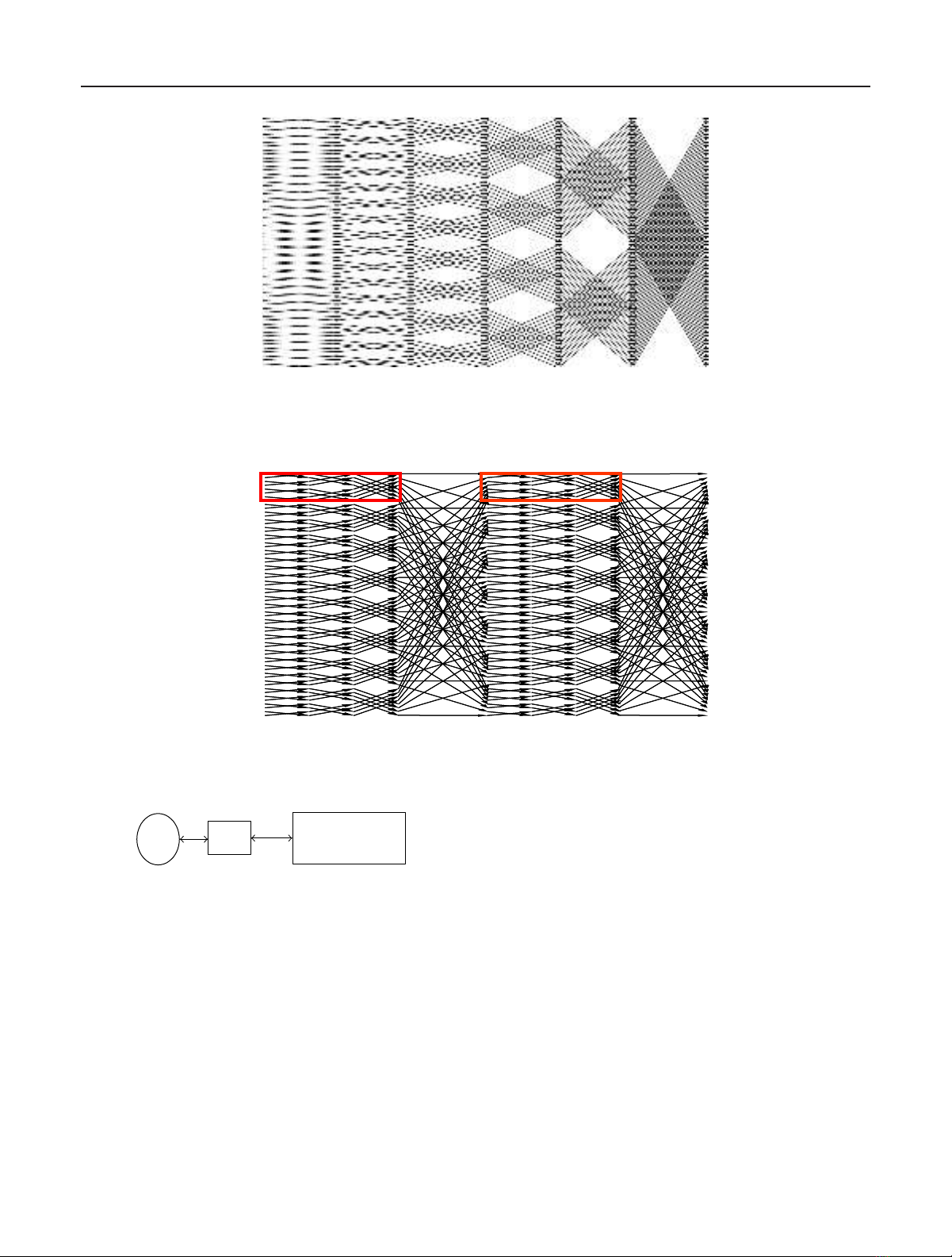
Figure 1 shows the traditional 64-point FFT dataflow di-
agram. We can see that the whole data are read and written
back to the main memory in every stage. As the FFT size in-
creases, stage number will be increased. As a result, the data
movement will cause much power consumption and long ex-
ecution time.
The basic idea of cached FFT is to reduce the number of
main memory access as shown in Figure 2.Insteadofpro-
cessing one stage of butterfly operation at a time, we store
data in local storage and process more data in one super-stage
(Pass0, Pass1, Pass2) at a period time. To achieve this, two sec-
tions of data movement operations differing from traditional
FFT are designed as shown in Figure 3. The resulting opera-
tions are still very regular and will not increase much com-
plexity. The data will read/write from the cache memory of
each super stage. Super stage can greatly reduce the number
of main memory access as the FFT size Nbecomes bigger.
The nomenclature of the cached FFT is defined by fol-
lowing stages [9].
(1) Stage. A stage is the part of an FFT where all Nmemory
locations are read, processed by a butterfly, and written
back once.
(2) Super stage. A super stage is the portion of the cached
FFT algorithm where all N-data word are loaded into a
cache, processed, and written back to the main mem-
ory once, which can be regarded as a super stage.
(3) Group. A group is the portion of a super stage where
a block of data is read from the main memory into a
cached, processed, and written back to the main mem-
ory.
(4) Pass. Apassistheportionofagroupwhereeachword
in the cache is read, processed with a butterfly, and
writtenbacktothecacheonce.
The detailed operations of the cached FFT are as follows.
(1) Input data are loaded into an N-word main memory.
(2) The number Cof the Nwords is assembled to a group.
The Cwords are loaded into the cache memory.
(3) The data in the cache are being processed by PE and
written back to cache. Repeat this step when all passes
in a super stage is processed.
(4) Processed data in the cache are flushed to main mem-
ory.
(5) Steps 2,3, and 4 are repeated until all Nwords have
been processed once in a super stage.
(6) Steps 2,3,4, and 5 are repeated till all super stages are
finished. Then the operation of the FFT is completed.
1308 EURASIP Journal on Applied Signal Processing
0
4
8
12
16
20
24
28
32
36
40
44
48
52
56
60
Stage 0 Stage 1 Stage 2 Stage 3 Stage 4 Stage 5
Figure 1: Traditional FFT dataflow diagram.
Pass 0 Pass 1 Pass 2 Pass 0 Pass 1 Pass 2
0
4
8
12
16
20
24
28
32
36
40
44
48
52
56
60
Super stage 0 Super stage 1
Figure 2: Cached FFT dataflow diagram [9].
PE Cache Memory
Figure 3: Cache-memory FFT processor architecture [9].
2.2. Proposed system architecture of the
variable-length FFT processor
Based on the design concept of the cached FFT, we propose a
variable-length FFT/IFFT processor architecture for OFDM
application communication systems. It consists of three de-
sign units: CLU, AG, and PE, as shown in Figure 4. The CLU
decides the forward/inverse FFT operation and the number
of points that FFT will perform, based on the control word.
The AG unit can generate the address that RAM and ROM
accesses need. With the address, the coefficient ROM can
output the twiddle factor to butterfly processing element.
Then the PE can perform the complex arithmetic operations
for the data of RAM and the coefficients stored in ROM. The
RAM will store the input data as well as the temporary com-
puted data and also play the role of the cache. The outputs of
the FFT/IFFT results are also stored in the RAM for access.
The following sections will discuss the design issues of those
major functional units.
3. PROCESSING ELEMENT (PE) DESIGN
The coordinate rotational digital computer (CORDIC) algo-
rithm is a well-known VLSI arithmetic unit. The basic con-
cept of CORDIC is to decompose the desired rotation angles
into several easy-to-be-implemented subangles [12,13,14].
The subangles can be implemented by the shift-and-add. In
the traditional FFT hardware implementation, it needs many
multipliers and adders to achieve the complex multiplica-
tions. This will always cause very large hardware require-
ment. In order to reduce the hardware complexity, many FFT
VLSI Design of a Variable-Length FFT/IFFT Processor 1309
Coeffici ent
ROM
Addres s
G enerating
Circuit
Access
C ontro l
Circuit
M ode
Selecting
Citcuit
B utterfly
Processing
Elem ent
Control logic
unit
Control
word
Mode
selecting
circuit
Address
generating
circuit
Coefficient
ROM
Access
control
circuit
RAM
Butterfly
processing
element
Data input/output
Figure 4: The proposed variable-length FFT/IFFT processor archi-
tecture.
processors have employed the CORDIC to perform twiddle
factor operations. In this work, we adopted the newly pro-
posed MSR-CORDIC scheme [10] to compose these suban-
gles. With these easy-to-be-implemented subangles, the ro-
tation operations can be performed easily. Besides, the hard-
ware requirement of CORDIC is very simple. It also has po-
tential advantage of low switching activity for low-power op-
erations.
3.1. Review of MSR-CORDIC algorithm
In the conventional CORDIC algorithm [12], the scaling fac-
tor is always greater than 1. Therefore, it is necessary to scale
down the norm of the input vector to its initial value af-
ter the rotation mode is finished. Furthermore, the signal-
to-quantization-noise ratio (SQNR) will be reduced due to
the growth of the scaling factor. To avoid the overhead of
the scaling operation, the product of the scaling factors must
be equal to 1. To overcome these problems, the range of the
scaling factors must be greater and less than 1. The MSR-
CORDIC algorithm [10] reformulates the iterative arith-
metic as in Algorithm 1,whereµi,µj∈{−1,0,1};Iand Jde-
note the number of SPT terms of x(n)andy(n), respectively,
and they are referred to as the extending factors;θnis the ele-
mentary angle and the initial value; pn+1 denotes the product
of the scaling factors in nth iteration. The initial value of p1
is 1; Nspt are denoted as the number of SPT terms used in
performing (1), which is the sum of Iand J;Ndenotes the
total number of iteration; sn∈{0,1,...,S}and Sdenotes the
number of maximum shift.
In the conventional CORDIC [12] and EEAS-CORDIC
[15] algorithm, the norms of both schemes are enlarged af-
ter the micro-rotation operations. That is, the norm is am-
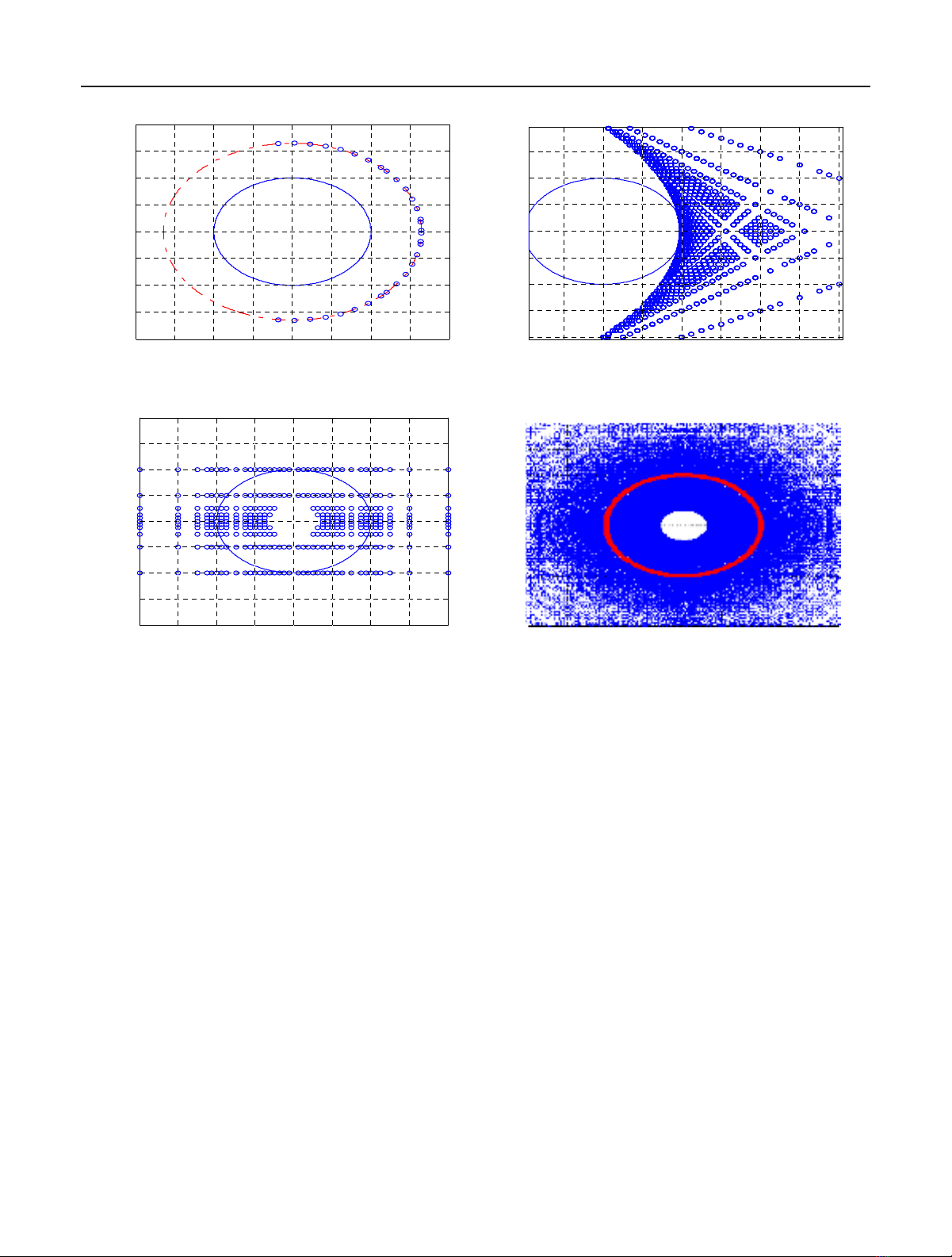
plified as illustrated in Figures 5a and 5b and Rm denotes
the total iteration number of CORDIC. On the contrary, in
MSR-CORDIC algorithm, (4) shows that the factor Pncan be
either greater or less than 1. In Figures 5c and 5d, we depict
the reachable points in 2D plane to emphasize the feature of
Pn.
For n=0,1,...,N
I. Rotation phase
x(n+1)
y(n+1)
=
J
j=1
µj2−sj−
I
i=1
µi2−si
I
i=1
µi2−si
J
j=1
µj2−sj
x(n)
y(n)
.(1)
•Elementary angle
θn+1 =tan−1
I
i=1µi2−si
J
j=1µj2−sj
.(2)
•Accumulation angle
z(n+1)=z(n)+θn+1.(3)
II. Scaling phase
•Scaling factor
pn+1 =
I
i=1
µi2−si
2
+
J
j=1
µj2−sj
2
.(4)
•Product of the scaling factor
pn+1 =pn×pn+1,(5)
End
Algorithm 1
From Figure 5, some other interesting features of the pro-
posed scheme are discussed below.
(1) According to (2), the angles in MSR-CORDIC is much
denser than the conventional CORDIC and EEAS-
CORDIC, hence, the MSR-CORDIC can reach the tar-
get angle with fewer iteration as shown in Figure 5d.
Furthermore, if we design the parameters, si,µi,ap-
propriately so that both the quantization error of ro-
tation angles and norms meet the system performance
requirement at the same time, then the scaling oper-
ation can be avoided. Since we do not need the extra
scaling operations, the MSR-CORDIC is faster in com-
putational speed and the corresponding hardware cost
is reduced.
(2) In some applications, the rotation angles are larger
than π/4, such as the twiddle factors in FFT. It is dif-
ficult for the conventional CORDIC to perform such
a rotation angle. In MVR-CORDIC [16], the authors
utilize the prerotation strategy to overcome the prob-
lem and have the improvement of error performance.
However, extra hardware costs and also the comput-
ing speed decrease. On the contrary, in the newly pro-
posed MSR-CORDIC algorithm, the reachable angles
are distributed from 0 to 2π.
1310 EURASIP Journal on Applied Signal Processing
2
1.5
1
0.5
0
−0.5
−1
−1.5
−2
−2−1.5−1−0.50 0.511.52
(a)
1.5
1
0.5
0
−0.5
−1
−1.5
−2
−0.50 0.511.52 2.53
(b)
2
1.5
1
0.5
0
−0.5
−1
−1.5
−2
−2−1.5−1−0.50 0.511.52
(c)
2
1.5
1
0.5
0
−0.5
−1
−1.5
−2
−2−1.5−1−0.500.511.52
(d)
Figure 5: Constellation of reachable points under the rotation process. (a) Conventional CORDIC with N=Rm =4. (b) EEAS-CORDIC
with maximum shift range S=4andRm=2. (c) MSR-CORDIC with I=2, J=1, and N=1. (d) MSR-CORDIC with I=2, J=1, and
N=2for1/3≦Pn ≦3 with maximum shift range S=4.
3.2. VLSI architecture of MSR-CORDIC for twiddle
factor operation
To realize the twiddle factor PE, we use the MSR-CORDIC-
based VLSI architecture as shown in Figure 6. In order to en-
hance the speed, we arrange two-level pipeline in CORDIC
design. The important differences from the conventional
CORDIC design are the parameter sequence arrangement,
physical consideration, and circuit speedup because of no-
scaling operations. Based on (2), both of x(n+1) and y(n+1)
are linear combination of their prior x(n)andy(n). All the
coefficients of x(n)andy(n)arepoweroftwonumberswith
the signs µiand µj, respectively. Hence, two Barrel shifter
arrays (BSAs) are used to perform shifting operations. The
number of the output signal is Nspt in each BSA. To perform
the summation of the outputs, 2(Nspt −1) add/subtract oper-
ations must be performed and 2(Nspt −1) adders/subtractors
are used or required to finish the process in one clock cycle.
Therefore, in each MSR-CORDIC module, only 2(Nspt −1)
additions/subtractions are required.
3.3. Low switching activity of PE unit
The switching activity of coefficient may cause much power
consumption in two’s complement representation system. In
CORDIC representation system, the representation of lower
switching activity can be achieved. In Figure 7, we can see the
different of switching activity between two’s complement and
CORDIC representations. The switching activity in CORDIC
representation is lower than two’s complement representa-
tion.
4. DESIGN OF ADDRESS GENERATOR UNIT
AND CONTROL LOGIC UNIT
4.1. Cached FFT/IFFT address generation [9]
For a traditional radix-rN-point FFT, the stage number is
S=logr(N). By closely examining the data access pattern,
we can recognize that butterflies are clustered into “Groups.”
We can represent the memory address by making use of two
virtual counters:


![Báo cáo seminar chuyên ngành Công nghệ hóa học và thực phẩm [Mới nhất]](https://cdn.tailieu.vn/images/document/thumbnail/2025/20250711/hienkelvinzoi@gmail.com/135x160/47051752458701.jpg)