
© 2015 WILEY-VCH Verlag GmbH & Co. KGaA, Weinheim 1887
wileyonlinelibrary.com
COMMUNICATION
High-Quality Black Phosphorus Atomic Layers by
Liquid-Phase Exfoliation
Poya Yasaei , Bijandra Kumar , Tara Foroozan , Canhui Wang , Mohammad Asadi ,
David Tuschel , J. Ernesto Indacochea , Robert F. Klie , and Amin Salehi-Khojin*
P. Yasaei, Dr. B. Kumar, M. Asadi,
Prof. A. Salehi-Khojin
Department of Mechanical and Industrial Engineering
University of Illinois at Chicago
Chicago , IL 60607 , USA
E-mail: salehikh@uic.edu
T. Foroozan, Prof. J. E. Indacochea
Department of Civil and Materials Engineering
University of Illinois at Chicago
Chicago , IL 60607 , USA
C. Wang, Prof. R. F. Klie
Department of Physics
University of Illinois at Chicago
Chicago , IL 60607 , USA
D. Tuschel
HORIBA Scientifi c
HORIBA Scientifi c Inc.
Edison , NJ 08820 , USA
DOI: 10.1002/adma.201405150
(2.98–9.3 MPa
1/2 ), and examined their performance for BP
exfoliation (see Section S1, Supporting Information). Initially,
a chunk of black phosphorous crystal (0.02 mg mL
−1 ) was
immersed into different solvents and was sonicated for 15 h
(total input energy – 1 MJ). We noticed that aprotic and polar
solvents such as dimethylformamide (DMF) and dimethyl sulf-
oxide (DMSO) are appropriate solvents for the synthesis of
atomically thin BP nanofl akes and can produce uniform and
stable dispersions after the sonication (see Section S2, Sup-
porting Information). The solutions were then centrifuged
and their supernatants were carefully collected by a pipette.
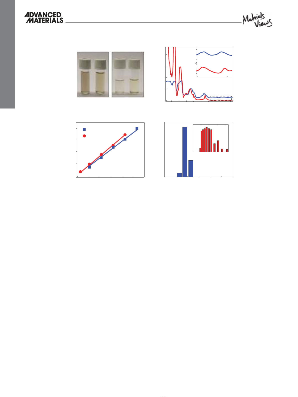
Figure 1 A shows the BP nanofl ake dispersions in DMSO and
DMF after sonication for 15 h (left image) and after the centrif-
ugation (right image), having concentrations up to 10 µg mL
−1
(see Experimental Section).
As suggested by experimental
[ 15 ] and theoretical
[ 16,17 ] reports,
BP atomic layers have a thickness dependent direct bandgap
ranging from ≈0.3 eV in bulk to more than 1 eV in monolayer.
Typically, optical absorption spectroscopy is a robust and reli-
able method to determine the bandgap of semiconductors in
solution form. We used this technique to characterize our dis-
persed nanofl akes in DMF and DMSO solutions with a focus
on the near-IR (NIR) range (Wavelength of 830–2400 nm)
where the peaks associated with the optical band gap of atomi-
cally thin BP nanofl akes are likely to occur. Interestingly, in
both DMF and DMSO solutions several spectral peaks were
observed in the NIR range at ≈1.38, ≈1.23, ≈1.05, ≈0.85, and
≈0.72 eV (labeled as numbers 1–5 in Figure 1 B) which are
believed to be associated with the enhanced light absorption by
mono-, to fi ve-layers thick BP nanofl akes, respectively. These
results are in a good agreement with the position of photolumi-
nescence peaks reported for mono- to fi ve-layers thick BP fl akes
obtained by mechanical exfoliation.
[ 12,22 ] The smaller peaks
at 1.38 and 1.23 eV compared to other peaks implies that the
yields of mono- and bilayers are lower than other atomic layers.
We also measured the normalized absorption intensity
over the characteristic length of the cell ( A / l ) at
λ
= 1176 nm
( E = 1.05 eV) for DMF and DMSO solutions at different con-
centrations ( C ). As suggested by the Lambert–Beer law
( A / l =
α
C , where
α
is the extinction coeffi cient), a linear trend
was observed for A / l versus concentration (Figure 1 C), sug-
gesting well-dispersed nanofl akes in both solutions. The extinc-
tion coeffi cients for DMF and DMSO solutions were extracted
to be
α
= 4819 and 5374 mL mg
−1 m −1 , respectively. The BP
fl ake size distribution was also analyzed by dynamic light scat-
tering (DLS) spectroscopy and the average fl ake sizes were
determined to be ≈190 and ≈532 nm for the DMF and DMSO
solutions, respectively (Figure 1 D).
2D nanomaterials such as graphene and transition metal dichal-
cogenides (TMDCs) have shown outstanding potential in many
fi elds such as fl exible electronics,
[ 1 ] sensing, [ 2,3 ] and optics,
[ 4 ]
due to their desirable physical and structural properties.
[ 5–7 ]
Among these materials, graphene has the highest charge car-
rier mobility,
[ 8 ] but absence of a bandgap limits its practice in
many applications.
[ 9 ] On the other hand, molybdenum disulfi de
(MoS
2 ) atomic layers offer a noticeable bandgap resulting in
extraordinary on/off ratios (>10
8 ), [ 10 ] but the material suffers
from moderate charge carrier mobility.
[ 11 ] Recent discovery
of black phosphorus (BP) atomic layers (called phosphorene)
holds promise to be widely used as an alternative 2D semicon-
ductor in many areas of electronics and optoelectronics, owing
to its high mobility,
[ 12–14 ] tunable direct bandgap,
[ 14–16 ] large on/
off ratios (>10
5 ), [ 13,14 ] and anisotropic properties.
[ 13,17,18 ] How-
ever, most of the studies on BP atomic layers so far
[ 12–15,19–21 ]
have used the mechanical exfoliation technique, which is only
suitable for laboratory level demonstrations. To harvest the
material’s excellent properties, it is essential to employ scal-
able techniques to produce large quantities of exfoliated nano-
fl akes. In this report, we employed the liquid-phase exfoliation
technique to produce highly crystalline atomically thin BP
nanofl akes in the solution form by using ultrasonic energy as
a source to break down the inter-layer van der Waals forces in
appropriate solvents (see Experimental Section).
We surveyed several solvents from different chemical fami-
lies such as alcohols, chloro-organic solvents, ketones, cyclic or
aliphatic pyrrolidones, N -alkyl-substituted amides, and orga-
nosulfur compounds, covering a wide range of surface ten-
sions (21.7–42.78 dyne cm
−1 ) and polar interaction parameters
Adv. Mater. 2015, 27, 1887–1892
www.advmat.de
www.MaterialsViews.com
1888 wileyonlinelibrary.com © 2015 WILEY-VCH Verlag GmbH & Co. KGaA, Weinheim
COMMUNICATION
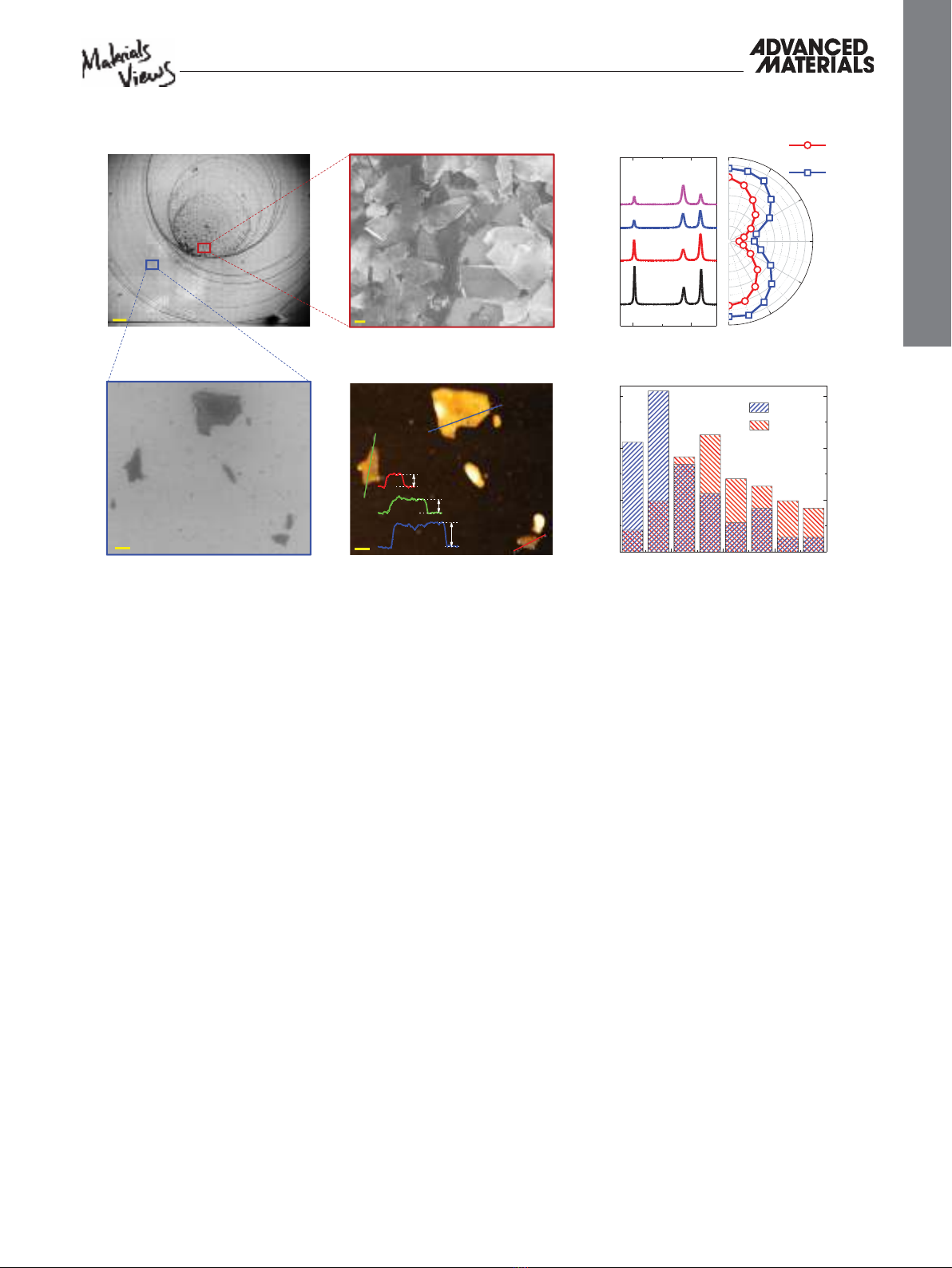
For further characterizations on isolated fl akes, we used the
“on chip separation method” in which the fl akes remain on the
surface in a circular pattern, due to the “coffee-ring effect”
[ 23 ]
( Figure 2 A). Higher-magnifi cation scanning electron micros-
copy (SEM) images show that the central area of the coffee
rings is densely packed by randomly oriented atomically thin
BP nanofl akes (Figure 2 B), while individual fl akes can be
easily found near the outer peripheral regions (Figure 2 D).
We collected Raman point spectra from the individual fl akes
and obtained typical Ag
1 (out-of-plane mode), B2g and Ag
2 (in-
plane modes) BP peaks at wavenumbers of ≈360, ≈437, and
≈466 cm
−1 , respectively (Figure 2 C). The peak positions are con-
sistent with the signature Raman spectrum of the mechanically
exfoliated BP fl akes, suggesting that the fl akes are crystalline
after the exfoliation.
[ 21 ] To investigate the anisotropic structure
of the exfoliated fl akes, we performed angle resolved Raman
spectroscopy experiments with a linearly polarized laser light.
Figure 2 C (left) shows the Raman point spectra obtained from
an individual BP fl ake at different sample orientations. Sim-
ilar to mechanically exfoliated fl akes,
[ 19,22,24 ] we observed that
the intensities of the three vibrational modes strongly depend
on the orientation of the sample. Figure 2 C (right) shows the
trend of Ag
1 and Ag
2 modes in 180° rotation of the sample.
According to structure of the BP, the A
g modes are expected to
be maximized when the laser polarization is aligned parallel to
the X-axis of the crystal.
[ 22 ] This can be used as a facile method
to determine the crystalline orientation of the fl akes.
[ 22 ]
The thickness distribution of the fl akes produced in DMF
and DMSO solutions was systematically investigated by per-
forming atomic force microscopy (AFM) height measurements.
Figure 2 D,E are SEM and AFM images of a randomly selected
region showing a variation in the thickness of the fl akes ranging
from 5.8 to 11.8 nm (Figure 2 E). Figure 2 F represents the his-
togram of the fl ake thickness distributions in DMF and DMSO
solutions obtained from height profi les of 70 individual fl akes.
In the case of DMF, >20% of the probed fl akes are thinner than
5 nm, while in DMSO the fl ake thicknesses are most frequently
in the range of 15–20 nm. Considering its higher yield of
atomic layers, we chose DMF for the rest of characterizations.
Next, we performed transmission electron microscopy
(TEM) characterization of the BP nanofl akes to study their
crystallinity, quality, and number of layers (see Experimental
Section and Section S4, Supporting Information). Figure 3 A
shows a typical TEM image of a BP nanofl ake on a lacy carbon
support. We used the fast Fourier transform (FFT) to iden-
tify the nanofl akes of BP with thicknesses down to a single
layer. As theoretically suggested,
[ 21 ] the intensity ratio of the
(110) to (200) diffraction peaks ( I 110 / I 200 ) is greater than one
Adv. Mater. 2015, 27, 1887–1892
www.advmat.de
www.MaterialsViews.com
0.6 0.8 1.0 1.2 1.4
0
150
300
1
2
5
4
A/L (m-1)
Energy (eV)
3
0369
0
20
40
α
DMF
1176
= 4819
α
DMSO
1176
= 5374
(ml.mg
-1
.m
-1
)
DMF
DMSO
A/L (m-1)
Concentration (
µ
g/mL)
AB
CD
0 200 400 600
DMSO
N.W. Intensity
Particle size (nm)
DMF
0 600 1200
1.2 1.4
2
4
18
20
DMSO
DMF
1
2
B
Sonicated Centrifuged
DMF DMSO DMF DMSO
Figure 1. Solution level characterization of liquid-phase-exfoliated BP nanofl akes. A) Photograph of the atomically thin BP dispersions in DMSO and
DMF solvents after sonication (left) and after centrifugation and supernatant collection (right). B) Optical absorption spectra obtained from dispersed
BP nanofl akes in DMSO and DMF solvents. Five peaks indicated by numbers 1–5 correspond to the optical bandgap of mono- to fi ve-layers BP nano-
fl akes. C) Normalized absorbance intensity over characteristic length of the cell ( A / l ) at different concentrations for
λ
= 1176 nm ( E = 1.05 eV). The
extinction coeffi cient (
α
) is extracted by linear fi tting and can be used to estimate concentration of the subsequent solutions. D) DLS histogram for
DMSO and DMF solution.
1889
wileyonlinelibrary.com
© 2015 WILEY-VCH Verlag GmbH & Co. KGaA, Weinheim
COMMUNICATION
for monolayer and smaller than one for multilayer. So far, this
ratio has only been experimentally verifi ed for multilayers.
[ 21 ]
In our images, the I 110 / I 200 ratio is measured to be 2.7 ± 0.2,
in good agreement with the computational value of 2.557
[ 21 ] for
monolayer BP (see Section S4.3, Supporting Information). In
Figure 3 B, the FFT patterns of different selected areas on dif-
ferent locations show identical features, suggesting the exist-
ence of a single crystalline, monolayer BP nanofl ake over the
whole image.
The atomic structure of the monolayer BP is resolved in
Figure 3 C using high-resolution TEM imaging. We also per-
formed TEM simulations (viewing from the (001) direction) on
mono- and multilayers BP structures using the well-known BP
lattice parameters.
[ 25 ] In the case of a monolayer, our simulated
image has a hexagonal structure similar to graphene, while
multilayers exhibit orthogonal structure due to ABA stacking
order in >1 layers (see Figure S8, Supporting Information).
The lattice parameters of simulated monolayer structure and
imaged fl ake perfectly matched, further confi rming the exist-
ence of monolayers. TEM image simulation (upper right inset)
and a fi ltered section of the acquired image (lower left inset) are
added to Figure 3 C for comparison.
The quality of the BP nanofl akes is analyzed by performing
energy-dispersive X-ray spectroscopy (EDX) analysis, as well
as electron energy loss spectroscopy (EELS). The EDX result
(Figure S10, Supporting Information) shows that the fl akes only
consist of phosphorous, without any noticeable impurity com-
ponents. EELS elemental mapping also shows that an entire
fl ake is only made of phosphorous atoms (Figure 3 D). The
near-edge fi ne structures of the phosphorous L
2,3 edges con-
fi rm the presence of pristine phosphorous and absence of the
signature P
x O
y peak loss (Figure 3 E).
[ 19 ] By repeating the EELS
analysis on the fl akes obtained from aged solution (1 month), it
was interestingly revealed that fl akes remain intact in solution
form. Panels A, B, and D of Figure 3 are taken from different
fl akes.
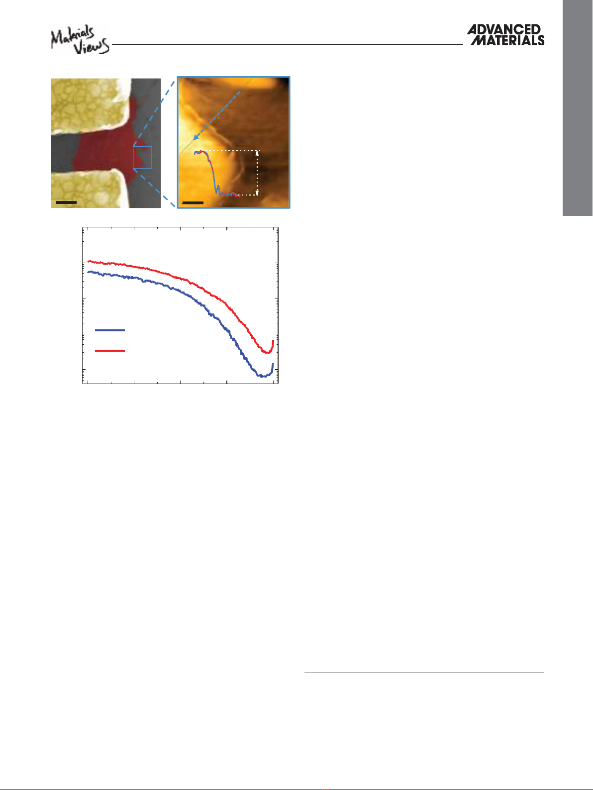
The electronic properties of individual BP nanofl akes were
characterized in a back-gated fi eld-effect transistor (FET) plat-
form. Figure 4 A shows the false color SEM image of a typical
fabricated device with a fl ake thickness of ≈7.4 nm as measured
by AFM (Figure 4 B). Figure 4 C shows the logarithmic scale
current versus back-gate voltage ( I SD vs V BG ) characteristics
of the device in ambient conditions at constant source-drain
bias ( V SD ) of 0.7 and 1.3 V. Using the linear slope of the I SD
Adv. Mater. 2015, 27, 1887–1892
www.advmat.de
www.MaterialsViews.com
360 450
90
o
0
o
60
o
30
o
A
2
g
B
2g
Intensity (a.u.)
Shift
(
cm
-1)
A
1
g
030
60
90
120
150
180
A1
g
A2
g
C
F
11.8 nm
6.8 nm
5.8 nm
E
B
A
D
0 10203040
0
10
20
30
Flake Frequncy (%)
Thickness (nm)
DMSO
DMF
Figure 2. Morphological and Raman characterization of the synthesized BP nanofl akes. A) Low magnifi cation SEM image of deposited nanofl akes
on SiO
2 /Si substrate, showing the “coffee-ring” structure (scale bar is 200 µm). B) Magnifi ed SEM image of the central area of the rings (scale bar is
200 nm). C) Raman spectra of exfoliated BP nanofl akes at different orientations relative to the incident laser polarization. Three distinct spectral peaks
were observed at ≈360, ≈437, and ≈466 cm
−1 , which correspond to the Ag
1, B2g, and Ag
2 BP peaks, respectively. The left image shows four spectra obtained
from an individual fl ake in different orientations. The right image shows the orientation dependent A
g
1 and Ag
2 peak intensities. The strong variation
in the peak intensity corresponds to anisotropic crystalline structure of the exfoliated fl akes. D) SEM image of individual BP nanofl akes located at the
outer region of coffee rings (scale bar is 200 nm). E) AFM image of the same area (shown in (D)), and their height profi les (inset) corresponding to
the drawn lines (same colors). F) Statistical fl ake thickness distribution measured by AFM on 70 fl akes, obtained from DMF and DMSO solutions
produced in identical experimental conditions.
1890 wileyonlinelibrary.com © 2015 WILEY-VCH Verlag GmbH & Co. KGaA, Weinheim
COMMUNICATION
versus V BG characteristics of the device ( V SD = 0.7 V) the fi eld-
effect mobility for holes is calculated to be ≈0.58 cm
2 V −1 s −1 .
The drain current modulation (on/off ratio) in our device is
as large as 10
3 . As shown in Figure 4 C, the n -branch starts at
V BG = 85 V which is in a good agreement with the previous
reports on FETs made of mechanically exfoliated BP fl akes in
similar gate conditions.
[ 13 ] The position of minimum conduc-
tivity can be shifted down by using thinner gate oxides,
[ 12 ] and
the electron mobility ( n -branch) can be enhanced using appro-
priate contact metals.
[ 26 ] The I SD – V SD characteristics of our
devices (provided in Section S5, Supporting Information) show
a non-Ohmic behavior, attributed to trap states and solvent
residues.
[ 27 ] The Schottky barrier and large contact resistances
are mainly responsible for the lower mobility values compared
with mechanically exfoliated BP FETs. Such transistors do not
often get to their saturation regime since a large portion of the
applied V SD drops across the contact resistances.
[ 12 ]
In summary, we have demonstrated large scale production of
highly crystalline and pure BP nanofl akes via liquid-phase exfo-
liation, where the dispersed fl akes are well protected against deg-
radation in the solution form. The exfoliated nanofl akes show
competitive electrical properties to mechanically exfoliated BP
fl akes. This work opens up new possibilities for the BP atomic
layers to be formed into thin fi lms and composites in large scales
with a wide range of applications such as fl exible electronics and
optoelectronics,
[ 1,28,29 ] energy generation and storage systems,
[ 30 ]
catalysis,
[ 31,32 ] chemical- [ 33 ] and biosensing,
[ 2 ] etc.
During the revision process of this paper we noted that
an experimental paper on liquid- phase exfoliation of BP was
published.
[ 34 ]
Experimental Section
Sample Preparation : Bulk black phosphorous (purchased from
Smart Elements) of ≈0.2 mg was immersed in 10 mL of solutions in
the form of either a single chunk, or a ground powder. The prepared
samples were sonicated in a Sonics Vibra-Cell sonicator (130 W)
for an appropriate time (see Section S3, Supporting Information for
the optimization process). Afterward, the solution was centrifuged
in an Eppendorf 5424 Centrifugation machine (250 W) for 30 min
in 2000 rpm and the top 50% of the solution was collected and
fi ltered using a Sigma–Aldrich vacuum fi ltration assembly on a
polytetrafl uoroethylene (PTFE) membrane fi lter of 0.1 µm pore size.
The fi ltered fi lm was then thoroughly washed many times by ethanol,
water, and isopropyl alcohol (IPA) to remove the solvent residue. The
stacked fl akes were then dispersed in IPA. The solution was drop cast
on degenerately doped Si substrate with 270 nm thermally grown SiO
2
using polyethylene pipette and dried under light (or on a hotplate at
90 °C). The samples were then gently rinsed in methanol, deionized
(DI) water, and IPA and N
2 blown to remove the solvent residues in
the evaporation stage.
UV–vis–IR Spectroscopy : UV–vis–NIR spectroscopy was performed
using a Perkin–Elmer LAMBDA 1050 high-performance UV/Vis/NIR
double-beam spectrophotometer. This machine covers the wavelength
range of 185–3300 nm using three detectors (photomultiplier R6872,
three-stage wide-band Peltier cooled InGaAs and single-stage Peltier
cooled PbS). We mainly focused on the NIR range using the InGaAs
detector, which covers the range of (≈830 to ≈2400 nm).
DLS : DLS was carried out at 25 °C using a DLS unit from Brookhaven
Instruments, which consists of a Brookhaven BI-200 goniometer and
BI-9000 high-speed correlator and a 3 W argon-ion laser operating at
514 nm. The volume of the samples was 50 µL. All the samples were
cleared of any air bubbles before measurement. The correlated nanofl ake
size was measured based on calculated base line with a 1–5% error.
SEM : SEM was performed using a Carl–Zeiss electron microscope
integrated in a Raith e-LiNE plus electron-beam lithography system. The
Adv. Mater. 2015, 27, 1887–1892
www.advmat.de
www.MaterialsViews.com
120 140 160 180
Energy Loss (eV)
Counts
(a.u.)
P L
2,3
E
3.27 Å
4.37 Å
2.83 Å
CD
monolayer
hydrocarbon
1
2
020
110
1-10
B
A
Figure 3. High-resolution TEM and EELS characterizations of BP nanofl akes. A) A typical TEM image of a BP fl ake on lacy carbon support (scale bar
is 200 nm). B) TEM image, as well as FFT of the selected area 1 (upper right) and 2 (lower right), showing monolayer BP covering a region in excess
of 80 nm × 80 nm (scale bar is 20 nm). The FFT patterns of different selected areas across the entire fl ake show identical features, suggesting uniform
existence of single layer BP over the entire fl ake. C) High resolution TEM image of monolayer BP nanofl ake taken from a selective area in B (scale bar
is 1 nm). TEM simulation (upper right inset) and a fi ltered section of the acquired image (lower left inset) are added for comparison. The lattice para-
meters perfectly match the monolayer BP structure. D) EELS map and corresponding high-angle annular dark-fi eld (HAADF) image (upper right inset)
of a fl ake on lacy carbon support (scale bar is 200 nm). Comparison between HAADF and spectrum images shows a pure phosphorous distribution
on the fl ake. Each pixel size of the EELS map is 22 nm. E) An individual EELS spectrum of the EELS map shown in D). Absence of the signature P
x O
y
peak loss confi rms the pristine phosphorous structure all over the fl ake. Panels (A), (B), and (D) are taken from different fl akes.
1891
wileyonlinelibrary.com
© 2015 WILEY-VCH Verlag GmbH & Co. KGaA, Weinheim
COMMUNICATION
images were acquired at 20 kV acceleration voltage and with a 30 µm
aperture size.
AFM : AFM was performed on drop-cast fl akes on Si/SiO
2 substrates
using an Icon Bruker system in standard tapping mode. It was tried to
minimize the time between sample preparation and AFM experiments in
order to reduce the degradation of the fl akes.
Raman Spectroscopy : The polarization/orientation Raman
measurements of the liquid exfoliated fl akes were performed using a
HORIBA XploRA instrument. The excitation wavelength was 532 nm
with 1.0 mW focused on individual fl akes of phosphorene using a 100×
microscope objective. Data were collected without a Raman analyzer.
Samples were mounted on a rotational stage with 15° rotational
gradations. The BP nanofl akes that appeared the most uniform based
upon their color when viewed with white refl ected light were selected
for polarization/orientation Raman analysis. This was done to avoid
convolution of spatially varying structural contributions to the spectra as
the sample’s orientation with respect to the incident laser polarization
was varied. Spectra were collected in 15° rotational increments from 0°
to 180° with respect to the laboratory frame.
TEM : The exfoliated fl akes were characterized in the aberration-
corrected JEOL ARM200CF scanning TEM (STEM)/TEM operated at
electron energy of 80 keV to minimize damage caused by the electron
beam. The microscope was equipped with a cold fi eld-emission source,
which yielded 0.35 eV energy resolution and 1.2 Å spatial resolution
with the probe spherical-aberration corrector in STEM mode, and 2 Å
resolution in TEM mode. A convergence semiangle of 16.5 mrad was
used for both STEM imaging and EELS. For HAADF-STEM imaging,
a 90 mrad collection inner angle was used. For EELS, a collection
semiangle of 71 mrad was used. A digital micrograph (Gatan, Inc.,
USA) was utilized for all data acquisition. For sample preparation, the
dispersed nanofl akes in IPA were drop-cast on a lacey-carbon TEM grid.
The samples were then lamped for 15 min to dry out the solvent and
immediately loaded into the microscope. High-resolution TEM images of
both mono- and multilayer BP were simulated using Kirkland multislice
code
[ 35 ] using the following TEM parameters: incident beam energy:
80 keV; thermal vibration temperature: 300 K; spherical aberration C s :
0.5 mm; defocus for single layer: 30 Å; defocus for multilayer: 48 Å;
objective aperture size: 500 mrad.
Device Fabrication and Electrical Measurements : The samples were
prepared using the drop-casting technique and were immediately
annealed at 200 °C for 2 h in vacuum to remove the excess residue
and increase the adhesion of the fl akes to the substrate. This step is
essential to reduce the contact resistance. The samples were then
immediately coated with a poly(methyl methacrylate) (PMMA) double
layer and the electrode patterns were carried out in an electron-beam
lithography (EBL) process. Immediately after developing, the samples
were loaded in a metal evaporation vacuum chamber and 15 nm of
titanium followed by 85 nm of gold were deposited. The samples were
annealed again in vacuum at 200 °C for 2 h to remove fabrication
residues. The samples were always kept in a vacuum except during
the electrical characterizations. The electrical performance of the
devices was monitored using Keithley 2612A source-meter in two-
probe confi guration. All the electrical measurements were carried out in
ambient conditions.
Supporting Information
Supporting Information is available from the Wiley Online Library or
from the author.
Acknowledgements
B.K. and T.F. contributed equally to this work. A.S.-K., P.Y., B.K., T.F.
conceived the idea. A.S.-K. led the material synthesis, fabrication,
characterizations (except TEM), and experiments. R.F.K. led the TEM
analysis and imaging. T.F., B.K., and M.A. performed the liquid exfoliation
and absorption spectroscopy experiments. M.A. performed DLS. P.Y.
performed SEM, AFM, device fabrication, and electrical characterizations.
D.T. and P.Y. performed Raman spectroscopy experiments. C.W.
performed TEM imaging and analysis. A.S.K. and J.E.I. jointly supervised
T.F. All the authors contributed to manuscript preparation and
discussions. A.S.-K.’s work was supported by the University of Illinois
at Chicago through the Startup budget. The acquisition of the UIC JEOL
JEM-ARM200CF is supported by a MRI-R2 grant from the National
Science Foundation [DMR-0959470]. The authors acknowledge the
MRSEC Materials Preparation and Measurement Laboratory shared user
facility at the University of Chicago (Grant No. NSF-DMR-1420709).
Received: November 10, 2014
Revised: December 26, 2014
Published online: February 2, 2015
[1] K. S. Kim , Y. Zhao , H. Jang , S. Y. Lee , J. M. Kim , K. S. Kim , J.-H. Ahn ,
P. Kim , J.-Y. Choi , B. H. Hong , Nature 2009 , 457 , 706 .
[2] Y. Shao , J. Wang , H. Wu , J. Liu , I. A. Aksay , Y. Lin , Electroanalysis
2010 , 22 , 1027 .
Adv. Mater. 2015, 27, 1887–1892
www.advmat.de
www.MaterialsViews.com
-100 -50 0 50 100
10
-3
10
-2
10
-1
10
0
10
1
V
SD
=0.7 V
V
SD
=1.3 V
I
SD
(µA)
V
BG
(V)
nm
7.4
BA
C
Figure 4. Electrical characterization of individual fl ake FETs and centi-
meter scale thin fi lm. A) False color SEM image of an individual few layers
thick BP FET. The scale bar is 200 nm. B) AFM image of selected region of
Figure 4 A. Line profi le corresponding to drawn line (blue) shows height
(7.4 nm) of the nanofl ake. The scale bar is 50 nm. C) Source–drain cur-
rent ( I SD ) with respect to the applied back gate voltage ( V BG ) swept from
−100 to +100 V. The source-drain bias ( V SD ) is 0.7 and 1.3 V for the black
and red curves, respectively.


%20--%3e%3cdefs%3e%3cstyle%3e%20.st0%20{%20fill:%20%23fff;%20}%20.st1%20{%20fill:%20%237800fa;%20}%20%3c/style%3e%3c/defs%3e%3cpath%20class='st1'%20d='M117.78,12.18H43.11c2.9,3.47,4.65,7.94,4.65,12.82,0,5.6-2.3,10.66-6.01,14.29h76.02l7.22-13.56-7.22-13.56Z'/%3e%3cg%3e%3cpath%20class='st0'%20d='M53.58,26.17h-.59v-1.46h.59v-4.96h2.83c1.78,0,2.67.94,2.67,2.82v5.76c0,1.87-.89,2.81-2.67,2.81h-2.83v-4.96ZM55.36,21.37v3.34h1.1v1.46h-1.1v3.34h1.01c.61,0,.91-.37.91-1.1v-5.93c0-.74-.3-1.1-.91-1.1h-1.01Z'/%3e%3cpath%20class='st0'%20d='M65.99,31.14h-1.8l-.31-2.07h-2.19l-.31,2.07h-1.64l1.82-11.39h2.62l1.82,11.39ZM65.28,18.04c-.25.46-.51.77-.75.94-.21.15-.47.22-.79.22-.26,0-.57-.07-.92-.22l-.38-.15c-.14-.05-.26-.07-.37-.07-.3,0-.53.18-.71.54l-.91-.68c.25-.46.51-.77.75-.94.21-.14.48-.21.79-.21.26,0,.57.07.92.21l.38.15c.14.05.26.07.37.07.3,0,.53-.18.71-.54l.91.68ZM61.91,27.52h1.73l-.87-5.76-.87,5.76Z'/%3e%3cpath%20class='st0'%20d='M74.53,26.89v1.52c0,1.91-.89,2.86-2.67,2.86s-2.67-.95-2.67-2.86v-5.93c0-1.91.89-2.86,2.67-2.86s2.67.95,2.67,2.86v1.11h-1.69v-1.22c0-.75-.31-1.12-.93-1.12s-.93.37-.93,1.12v6.15c0,.74.31,1.11.93,1.11s.93-.37.93-1.11v-1.63h1.69Z'/%3e%3cpath%20class='st0'%20d='M81.4,31.14h-1.8l-.31-2.07h-2.19l-.31,2.07h-1.64l1.82-11.39h2.62l1.82,11.39ZM75.9,19.2l1.52-1.91h1.71l1.51,1.91h-1.61l-.76-.95-.75.95h-1.61ZM77.32,27.52h1.73l-.87-5.76-.87,5.76ZM83.1,15.99l-1.76,1.91h-1.26l1.17-1.91h1.86Z'/%3e%3cpath%20class='st0'%20d='M84.86,19.75c1.78,0,2.67.94,2.67,2.82v1.48c0,1.87-.89,2.81-2.67,2.81h-.85v4.28h-1.79v-11.39h2.64ZM84.01,21.37v3.86h.85c.58,0,.87-.36.87-1.08v-1.71c0-.71-.29-1.07-.87-1.07h-.85Z'/%3e%3cpath%20class='st0'%20d='M93.51,19.75c1.78,0,2.67.94,2.67,2.82v1.48c0,1.87-.89,2.81-2.67,2.81h-.85v4.28h-1.79v-11.39h2.64ZM92.66,21.37v3.86h.85c.58,0,.87-.36.87-1.08v-1.71c0-.71-.29-1.07-.87-1.07h-.85Z'/%3e%3cpath%20class='st0'%20d='M98.8,31.14h-1.79v-11.39h1.79v4.88h2.03v-4.88h1.83v11.39h-1.83v-4.88h-2.03v4.88Z'/%3e%3cpath%20class='st0'%20d='M105.36,24.55h2.46v1.62h-2.46v3.34h3.09v1.63h-4.88v-11.39h4.88v1.63h-3.09v3.18ZM108.17,17.29l-1.76,1.91h-1.26l1.17-1.91h1.86Z'/%3e%3cpath%20class='st0'%20d='M112.2,19.75c1.78,0,2.67.94,2.67,2.82v1.48c0,1.87-.89,2.81-2.67,2.81h-.85v4.28h-1.79v-11.39h2.64ZM111.35,21.37v3.86h.85c.58,0,.87-.36.87-1.08v-1.71c0-.71-.29-1.07-.87-1.07h-.85Z'/%3e%3c/g%3e%3ccircle%20class='st1'%20cx='25'%20cy='25'%20r='20'/%3e%3cpath%20class='st0'%20d='M32.78,19.27c2.92,0,4.43,2.55,5.28,5.33l.71,2.17c.14.38-.33.75-.71.75h-5.61c.19-.33.24-.71.09-1.08l-.75-2.45c-.43-1.32-.99-2.64-1.79-3.77.75-.57,1.65-.94,2.78-.94h0ZM25,18.38c3.25,0,4.9,2.78,5.89,5.89l.76,2.45c.14.42-.33.8-.8.8h-11.69c-.42,0-.94-.38-.8-.8l.75-2.45c.99-3.11,2.64-5.89,5.89-5.89h0ZM25,11.35c1.74,0,3.11,1.37,3.11,3.11s-1.37,3.11-3.11,3.11-3.11-1.41-3.11-3.11,1.41-3.11,3.11-3.11h0ZM17.27,19.27c1.08,0,1.98.38,2.73.94-.8,1.13-1.37,2.45-1.74,3.77l-.8,2.45c-.14.38-.05.75.09,1.08h-5.56c-.42,0-.9-.38-.75-.75l.71-2.17c.9-2.78,2.41-5.33,5.33-5.33h0ZM17.27,12.91c1.51,0,2.78,1.27,2.78,2.83s-1.27,2.83-2.78,2.83-2.83-1.27-2.83-2.83,1.27-2.83,2.83-2.83h0ZM32.78,12.91c1.56,0,2.78,1.27,2.78,2.83s-1.23,2.83-2.78,2.83-2.83-1.27-2.83-2.83,1.27-2.83,2.83-2.83h0ZM27.07,28.56v.09c0,.57-.24,1.08-.61,1.46h0v.05c-.38.33-.9.57-1.46.57s-1.08-.24-1.46-.61h0c-.38-.38-.61-.9-.61-1.46v-.09h1.41v.09c0,.19.05.38.19.47v.05c.09.09.28.19.47.19s.38-.09.47-.19v-.05c.14-.09.24-.28.24-.47t-.05-.09h1.41ZM30.99,28.56v.09c0,1.65-.66,3.16-1.74,4.24-1.08,1.08-2.59,1.79-4.24,1.79s-3.16-.71-4.24-1.79l-.05-.05c-1.04-1.08-1.7-2.55-1.7-4.2v-.09h1.41v.09c0,1.27.47,2.4,1.27,3.25h.05c.85.85,1.98,1.37,3.25,1.37s2.4-.52,3.25-1.37c.85-.8,1.37-1.98,1.37-3.25v-.09h1.37ZM34.99,28.56v.09c0,2.78-1.13,5.28-2.92,7.07-1.79,1.79-4.29,2.92-7.07,2.92s-5.23-1.13-7.07-2.92c-1.79-1.79-2.92-4.29-2.92-7.07v-.09h1.41v.09c0,2.4.94,4.53,2.5,6.08,1.56,1.56,3.72,2.5,6.08,2.5s4.52-.94,6.08-2.5c1.56-1.56,2.5-3.68,2.5-6.08v-.09h1.41Z'/%3e%3c/svg%3e)