
Dung Truong Cao, Hien Nguyen Trung, Duy Nguyen Thi Hang, Thuy Tran Thi Thanh
Abstract— This paper presents the operating principle
of a 1×2 optical router and the numerical simulation design
of its constituent components. The optical router comprises
arrayed waveguide grating (AWG) structures, waveguide
Bragg gratings (WGBG), a 1×2 optical switch utilizing 2×2
multimode interference (MMI) couplers, and wavelength-
selective routing based on microring resonators for six
high-density wavelength channels in dense wavelength-
division multiplexing (DWDM) applications.
Computational results from localized simulations for each
component demonstrate excellent optical performance,
validating the adherence to the design principles. These
favorable outcomes indicate significant potential for the
proposed structure in high-density wavelength-selective
routing devices for DWDM optical communication
systems and high-speed optical interconnects.
Keywords— optical router, arrayed waveguide grating
(AWG), Bragg grating waveguide, microring resonator,
numerical simulation, silicon photonics.
I. INTRODUCTION
Due to the explosive increase in the number of mobile
terminal devices and the rapid development of multimedia
applications and cloud computing services, the demand for
transmission capacity and network bandwidth in optical
networks has grown exponentially. Wavelength-division
multiplexing (WDM) technology has emerged as the most
widely used solution to meet the ever-increasing
bandwidth requirements[1]–[3]. An essential device in
WDM networks is the optical add-drop multiplexer
(OADM). It can selectively remove/add one or more
wavelength channels at a network node without the need
for costly optical-electrical-optical (OEO) conversions.
In a WDM system, the waveguide routing is arranged in
an Arrayed Waveguide Grating (AWG) array, acting as a
key component. The AWG is specifically designed for
channel multiplexing and demultiplexing, separating
optical signals into individual wavelength channels. The
AWG consists of an array of optical waveguides, which are
typically planar structures that guide the optical signals.
These waveguides are often designed to support a specific
wavelength or range of wavelengths. WDM technology,
with the help of AWGs, significantly increases the capacity
of optical communication systems. By utilizing different
wavelengths to carry distinct signals simultaneously,
WDM allows for a higher data transmission capacity over
a single optical fiber. Today, AWG (Arrayed Waveguide
Grating) configurations offer flexibility in the management
and upgrading of optical networks. Wavelength channels
can be added or removed in a flexible manner. AWG also
allows for high-density support of multiplexing and
demultiplexing with channel spacing, for example, at
intervals such as 0.2 nm, 0.4 nm, and 0.8 nm, in compliance
with the ITU-T G.694.1 standard grid, ensuring high
performance.
Additionally, in the planar waveguide technology, Bragg
gratings have been utilized in various applications such as
filters, dispersion compensation, pulse shaping [4], and
more. Recently, the integration of Bragg grating
waveguides on the silicon-on-insulator (SOI) platform has
garnered increasing research interest. Narrow-band Bragg
gratings prove highly useful in many applications, such as
wavelength-division multiplexing (WDM) channel filters.
To confine a narrow bandwidth, it is necessary to construct
longer Bragg gratings with weak coupling. Bragg grating
nano-waveguides exhibit strong mode confinement with
disorder along the sidewalls, resulting in large coupling
coefficients, even with bending amplitudes of only a few
nanometers. To mitigate the coupling coefficient, spatially
periodic refractive index disorder is placed away from the
grating waveguide [5] or built on the sidewalls of the slab
waveguide [6]. Since these are two-port devices, a 2 × 2
mode-selective coupler [7], asymmetric Y-branch [8], or
adiabatic taper coupler [9] is required to eliminate Bragg
reflection. However, achieving precise fabrication for such
devices remains challenging.
A wavelength-routed optical router plays a crucial role
in information systems based on Wavelength Division
Multiplexing (WDM) technology, such as WDM fiber
optic systems or high-speed optical interconnects in
network-on-chip (NoC) optical systems. Some studied
proposals of photonic integrated devices for optical
wavelength router based on microring resonators allow to
add/drop the optical wavelengths selectively, however,
such structures require complex designs and need to be
equipped with waveguide crossings elements [10]. Some
configurations involve arrays of AWG matrices forming a
sequence and permuting the order of wavelengths,
resulting in inflexible configurations[11].
Dung Truong Cao, Hien Nguyen Trung, Duy Nguyen Thi Hang, Thuy Tran Thi Thanh
Posts and Telecommunications Institute of Technology
OPTICAL ROUTER UTILIZING
WAVEGUIDES COMBINED WITH BRAGG
GRATINGS ON SILICON PHOTONIC
Contact author: Dung Truong Cao
Email: dungtc@ptit.edu.vn
Manuscript received: 11/2023, revised: 12/2023, accepted:
01/2024.
SOÁ 01 (CS.01) 2024
TAÏP CHÍ KHOA HOÏC COÂNG NGHEÄ THOÂNG TIN VAØ TRUYEÀN THOÂNG 64
OPTICAL ROUTER UTILIZING WAVEGUIDES COMBINED WITH BRAGG GRATINGS ON SILICON PHOTONIC
This paper presents a design study of a wavelength-
routed optical router based on flat waveguide components
on the Silicon-on-Insulator (SOI) platform compatible with
CMOS fabrication processes. The design incorporates
Arrayed Waveguide Gratings (AWG), Bragg scattering
gratings, and is assisted by resonant ring couplers. The
paper primarily focuses on the design principles of the
AWG subsystem and the Bragg scattering gratings
combined with microring resonators for wavelength-
selective processing with six wavelengths following the
standard ITU-T G.694.1 grid. The components were
designed using the optical structure design tools BPM,
GratingMode and FullwaveFDTD within the commercial
software Rsoft.
II. STRUCTURAL DESCRIPTION AND
ELEMENTAL DESIGN
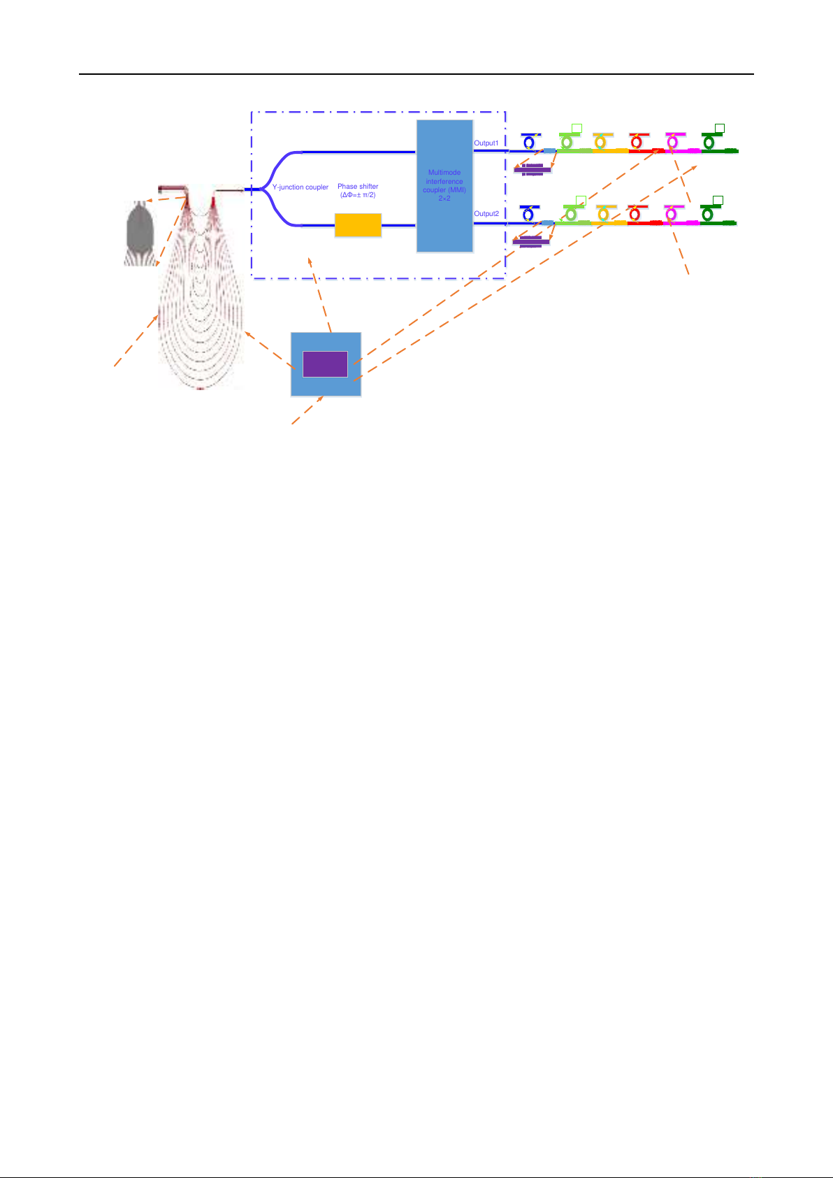
Figure 1 illustrates the operational principle of an optical
router for 6 channels conforming to the ITU-T G.694.1 grid
with a channel spacing of 0.8nm and the first wavelength
at 1549.32nm (corresponding to a frequency spacing of
100GHz and a central frequency of the first channel at
193.5THz). The structural system of the optical routing
device consists of three main components, including a
Wavelength Division Multiplexing (WDM) channel
coupler using two Arrayed Waveguide Grating (AWG)
structures for constructing a wavelength multiplexer, an
Optical Waveguide Switch (OWS) switch, and a
wavelength-selective demultiplexer based on Bragg
scattering gratings combined with microring resonators.
All elements in this investigation are designed for the
transverse electric (TE) polarization state and based on
channel waveguides fabricated from the standard silicon-
on-insulator (SOI) wafer with the thickness of the silicon
core layer of 220nm.
Initially, a system comprises 6 single-mode waveguides
guiding 6 individual input wavelengths at 1549.32 nm,
1550.12 nm, 1550.92 nm, 1551.72 nm, 1552.52 nm, and
1553.32 nm with the wavelength spacing as much as 0.8nm
corresponding to the frequency spacing of 100GHz,
respectively. Subsequently, these 6 wavelengths pass
through an AWG structured as an arrayed waveguide with
6 input ports and 15 output ports. Next, a star coupler
connects these 15 waveguides to another AWG with 15
input ports and 1 output port. Thus, a system with two
back-to-back configured AWGs creates a 6-channel
wavelength multiplexer.
Next, a 1×2 switchable optical waveguide structure
(OWS) consists of one input port and two output ports. The
input port of this OWS structure initially passes through a
symmetrical Y-junction coupler to split the incoming
optical signal into two branches. Subsequently, two arms
travel along two straight waveguides, with the lower
branch passing through a phase shifter utilizing the thermo-
optic effect generated by a thin metal film (Titanium metal)
placed above a waveguide. Then, these two branches pass
through a 2×2 multimode interference coupler (MMI) to
combine the optical signals, creating the expected 1×2
switch mechanism. The 2×2 MMI interference coupler
operates with 2 inputs and 2 outputs positioned at ±WMMI/4
(where WMMI is the width of the MMI waveguide, and the
coordinate axis is calculated along the vertical centerline of
the MMI waveguide). The length of the MMI coupler is
determined by:
3 / 2
MMI
LL
=
(1)
λ1λ2λ3λ4λ5λ6
SiO2
Silicon (Si)
Star waveguide coupler
Arrayed waveguide
grating (AWG)
Silicon microring
resonator
Silicon channel
waveguide
Six wavelength
channels (inputs) Six wavelength
channels (output) Multimode
interference
coupler (MMI)
2×2
Output1
Output2
λ1λ2λ3λ4λ5λ6
Silicon microring
resonator
Phase shifter
(ΔΦ=± π/2)
Y-junction coupler
1×2 Optical waveguide switch
(OWS)
SiO2 substrate
Figure.1. The principle design diagram of the optical router based on mode conversion and total internal reflection
in silicon waveguides.
SOÁ 01 (CS.01) 2024
TAÏP CHÍ KHOA HOÏC COÂNG NGHEÄ THOÂNG TIN VAØ TRUYEÀN THOÂNG 65

Dung Truong Cao, Hien Nguyen Trung, Duy Nguyen Thi Hang, Thuy Tran Thi Thanh
where
2
4
3
ee
nW
L
=
is the half-beat length of the MMI
coupler,
( )
-1/ 2
22
-
e MMI e c
W W n n
=+
TE polarization mode.
Before connecting to the 2×2 MMI coupler, we place a
controllable phase shifter with a suitable phase-shift to
perform a mode demultiplexer’s function by combing the
optical fields from two access arms. The 2×2 MMI coupler
in this design has the length
13 / 2
MMI
LL
=
, leading to its
transfer matrix is defined by [12]:
1
1
1
1
2
j
Mj
=
(2)
Hence, if the phase shifter has the phase difference
ΔΦ=±π/2, the 2×2 MMI coupler will combine two optical
paths from two arms of its input ports to the selectable
outputs of the 2×2 MMI coupler.
Then, a waveguide Bragg grating (WGBG) based on a
Bragg grating modulation scheme consists of a periodically
modulated refractive index structure along the core of a
single-mode optical waveguide. This modulation can either
be in the form of a narrow-band modulation of the edge-
relief type or a toothed comb-like modulation with an
apodization profile in a uniform or cosine-shaped fashion.
The entire waveguide structure is fabricated from a
standard silicon-on-insulator (SOI) wafer, providing
compatibility with Very Large-Scale Integration (VLSI)
CMOS fabrication technology. When a broad-spectrum
source is input, it produces a narrow-wavelength-reflected
spectrum with resonant wavelengths known as Bragg
wavelengths. The transmitted spectrum towards the output
exhibits missing wavelengths corresponding to the Bragg
wavelengths
B
l
. According to Bragg's law, the Bragg
diffraction method based on dielectric or pure
semiconductor waveguides (such as silicon, for example)
will only reflect a specific wavelength known as the Bragg
wavelength, determined by the formula [13]:
2eff
B
n
m
l
=
(3)
Here,
is the Bragg wavelength, and neff is the effective
refractive index of the waveguide core in optical
diffraction, and m=1,2,3... represents the diffraction order,
resonant order, or grating order. The operating principle of
the waveguide Bragg diffraction is similar to that of fiber
Bragg grating (FBG) diffraction.
The wavelength spacing between the first minima
(refer to Figure 2), or bandwidth
l
, is determined by the
refractive index modulation structure (as a transforming
function) given by the equation:
2
B
nh
ll
p
=
(4)
For the case of WGBG with width-modulated
apodization or height-modulated apodization, the
bandwidth
l
is determined according to the mode
coupling theory by [14],[15]:
( )
22
2/
B
g
L
n
l
l k p
p
= +
,
( )
22
12
0eff
nn
n
kl
−
=
(5)
where
B
l
is the resonant reflection wavelength
following the Bragg’s law,
g
n
is the group velocity
propagating into the grating,
k
is the coupling coefficient
of the grating, L is the length of the grating. The strength
of the coefficient
k
depends on the overlapping coefficient
(also called as mismatched coefficient)
. For TE-
polarized waves, solving the Maxwell's equations for
guided waves in the waveguide Bragg grating yields a
transcendental equation [14],[15] :
1/2
2
2
tan 4
V
v v v
=−
, với
( )
1/2
2 2 2
01
2
w
v k n b=−
, (6)
where,
0
0
2
kp
l
=
is the wavenumber in vacuum (free space)
with the operation wavelength
0
l
, the parameter V is
determined by:
( )
1/2
22
0 1 2
V k w n n=−
, w is the core width of
the grating. Reflectivity R of the waveguide grating at the
Bragg’s resonant wavelength is determined by:
22
2
2 2 2
sinh
cosh sinh
4
L
R
LL
kg
g g g
=
+
, with
2
22
4
gk
=+
(7)
In which, the coupling coefficient
k
at the Bragg
wavelength is followed as [16]:
( )
12
2
B
B
nn
kk l
−
==
(8)
Note that light diffraction of the grating occurs on a very
small scale, typically
B
l
around 1 μm. Therefore, this
property also makes diffraction highly beneficial in optical
fiber communication systems.
Diffraction gratings are created in a comb-like pattern
horizontally using electron beam lithography or extremely
ultraviolet photolithography (EUV) with a periodic
variation of δw = 1nm. The diffraction period is fixed at
= 0.005 μm with a sinusoidal grating profile. The grating
is formed with a uniform apodized aperture. It can also be
modulated by varying the core refractive index using
germanium doping into the silicon core. However, in this
study, we only consider the geometrically uniform
diffraction structure. By designing diffraction structures
with appropriate grating periods to achieve Bragg
reflection at 6 selected wavelengths.
Finally, in a scenario of practical applications to filter
the reflected wavelengths into separate channels in
individual single-mode waveguides, we employ a resonant
coupler combined with a diffraction structure to isolate
each wavelength individually. According to the theory of
resonant coupling, the mode matching between a straight
waveguide and a loop (with radius r) having equal
waveguide width (both in width and height within the
waveguide structure) leads to the condition for resonant
coupling when there is appropriate matching of the
waveguide moments, given by [17]:
SOÁ 01 (CS.01) 2024
TAÏP CHÍ KHOA HOÏC COÂNG NGHEÄ THOÂNG TIN VAØ TRUYEÀN THOÂNG 66
OPTICAL ROUTER UTILIZING WAVEGUIDES COMBINED WITH BRAGG GRATINGS ON SILICON PHOTONIC
mλm=2πrneff (9)
Here m is the mode number of the loop, λm corresponds to
the resonant wavelength of the mth mode, r is the radius of
the loop, neff is the effective refractive index of the loop
corresponding to the wavelength λm, and it depends on the
waveguide width, the gap g, which is the coupling gap
between the straight waveguide and the microring
waveguide.
According to the theory of coupled-ring resonators, a
coupled-ring resonator structure consists of a resonant ring,
which is a ring-shaped waveguide (ring resonator) coupled
with two straight waveguides oriented in parallel with
separation gaps denoted as g1 and g2. The coupling
coefficients due to the electric field interaction are denoted
as k1 and k2, respectively. The loss coefficient of the ring
resonator due to curved bend scattering and absorption is
denoted as α, the insertion loss coefficient due to the
straight waveguides is denoted as γ, and the radius of the
coupled-ring resonator is denoted as r. In this case, the
transfer function of the output (drop port) and input (input
port) fields is determined by the equation [18]:
11
22
11
exp( )
1 1 1 exp ( )
d
i
k k D j
E
Ek k j
cf
cf
−
=− − −
(10)
where
( )
1/2
1D=−g
,
( )
.exp / 4DL=−ca
,
2Lr=p
,
2/
eff
Ln=f p l
, λ is the operation wavelength into the
channel waveguides.
In symmetric design conditions, we set g1=g2=g, where
the structures are identical in geometry and geometric
symmetry. Consequently, k1=k2=k. The equations above
aid in designing the coupled-ring resonator as a switch and
help identify the optimal values for different parameters.
By adjusting the radius of the microresonator, we
resonate successively with each of the 6 selected
wavelengths. This allows us to selectively route and drop
each wavelength into dedicated single-mode waveguides.
In this way, we conclude the process of path selection and
add/drop functions of the designated wavelengths within
the desired ITU grid.
III. NUMERICAL SIMULATION DESIGN OF
ELEMENTS FOR THE PROPOSED ROUTER
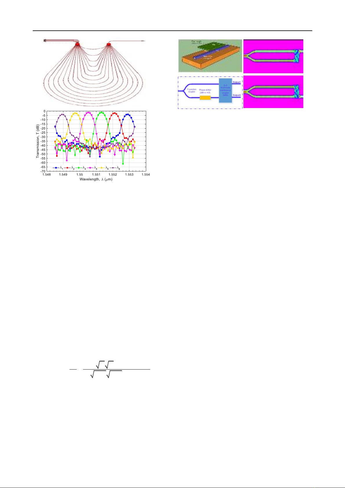
Firstly, we design a six-channel multiplexer using AWGs
based on channel waveguides with a silicon core and a
silica glass (SiO2) cladding. The refractive indices of the
core and cladding are 3.465 and 1.45, respectively, at a
wavelength of 1550nm. The width of the single-mode
waveguide at the input and output is designed to guide
independent wavelengths for the six selected wavelengths,
and the output waveguide width for the combined spectrum
of the six wavelengths is set to w=0.5μm (for single-mode
guidance). To design the wavelength division multiplexer,
we utilize the AWG Router tool in the commercial Rsoft
software. This tool allows for the automatic design of the
primary AWG waveguide structure using a reflective
grating-type configuration with an initial converging lens
structure at the input. Subsequently, the output ports are
connected back-to-back to a secondary AWG structure
with single-mode waveguides connected in a star coupler
configuration. The output of the secondary AWG serves as
a single output port for the spectrum of the 6 wavelengths.
Figure 2(a) illustrates the CAD-assisted design of the
structure, and Figure 2(b) shows the transmission
characteristics of the combined spectrum of the 6
wavelengths. It is observed that the wavelength
multiplexer enables high-density combining (channel
spacing of about 100 GHz) with low crosstalk, as the noise
signals are consistently lower than the peak signals of each
wavelength by more than 30 dB. Next, we design an optical
waveguide switch (OWS) structure in a 1×2 configuration.
This structure consists of a single-mode input waveguide.
A symmetrical Y-junction coupler, comprising sinusoidal
waveguides, is used to split the optical path in a 50:50 ratio.
(a)
(b)
Figure.2. (a) Schematic design of AWGs with star
couplers for creating a 6-channel DWDM multiplexer,
(b) transmission response of the wavelength spectrum
of the selected wavelength multiplexer.
(c)(a)
(d)
2×2
Multimode
interference
coupler
(MMI)
Output1
Output2
Phase shifter
(ΔΦ=± π/2)
Y-junction
coupler
1×2 Optical waveguide switch
(OWS)
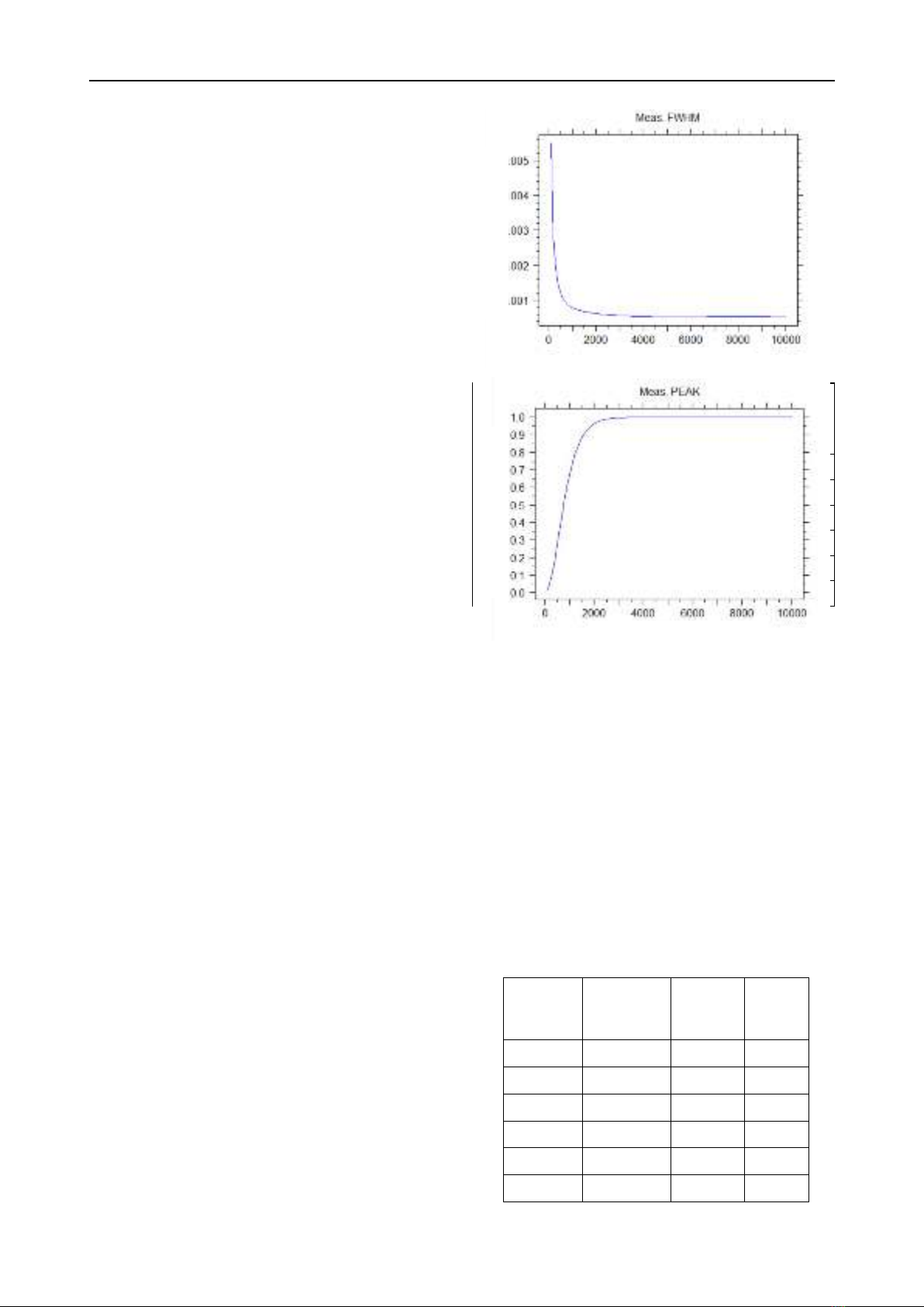
(b)
Figure.3. (a) structure diagram of the thermo-optic
phase shifter (TOPS), (b) placement of TOPS in the
1×2 OWS structure, (c) 3D-BPM electric field pattern
simulation for the phase shift ΔΦ = π/2, and (d) 3D-
BPM electric field pattern simulation for the phase
shift ΔΦ = -π/2.
SOÁ 01 (CS.01) 2024
TAÏP CHÍ KHOA HOÏC COÂNG NGHEÄ THOÂNG TIN VAØ TRUYEÀN THOÂNG 67
Dung Truong Cao, Hien Nguyen Trung, Duy Nguyen Thi Hang, Thuy Tran Thi Thanh
Subsequently, these two waveguides are straightened, and
one arm is equipped with a phase shifter to control the
switching. The phase shifter (PS) consists of a thin titanium
film placed above the waveguide, acting as a resistive
heater, separated from the waveguide by approximately 1
µm and powered by a direct current (DC) source in pulse
form. Under the influence of a pulsed DC source, the
Titanium metal thin film heats up and provides a localized
hot spot beneath the waveguide. The heat source alters the
refractive index of the silicon core in the thermal transition
region, inducing an optical phase shift ΔΦ as a function of
temperature. Subsequently, the two straight waveguides
are connected to a 2×2 multimode interference coupler
(MMI) at positions ±WMMI/2. This multimode coupler is
designed with a length as
13 / 2
MMI
LL
=
to produce the
corresponding phase matching in accordance with the
transfer matrix in Equation (2). Therefore, if the phase shift
ΔΦ=±π/2, the MMI coupler allows the combination of two
optical paths into a selected optical signal at one of the two
outputs, effectively creating a switching mechanism [12].
In this study, the width of the 2×2 MMI waveguide is
chosen as WMMI=3.8 µm, and the optimal length for the 2×2
MMI coupler to function as a perfect 3-dB coupler is
determined to be
13 / 2
MMI
LL
=
=56.8µm by using the 3D-
BPM simulation tool in the Rsoft software. Figure 3(a)
illustrates the structure of the Thermo-Optic Phase Shifter
(TOPS), Figure 3(b) shows the placement of TOPS in the
1×2 OWS structure, and Figures 3(c, d) represent the
simulation results obtained using the 3D-BPM method
corresponding to phase shifts ΔΦ = π/2 and ΔΦ = -π/2,
respectively.
Finally, a numerical simulation design for a wavelength
filter based on the WGBG structure is proposed and
simulated. Initially, the WGBG structure is considered as a
channel waveguide structure. Gratings are created through
a toothed comb pattern in the transverse direction using
electron beam lithography or extremely ultraviolet (EUV)
photolithography. The grating period is fixed at
=0.005
μm with sine-shaped grating profile. The grating structure
is apodized uniformly. The grating can also be modulated
by varying the refractive index of the core by incorporating
germanium into the silica core. However, in this study, we
only consider the grating structure that is geometrically
apodized. This is compatible with the CMOS process for
fabricating waveguides from standard SOI wafers (220nm
Si core thickness on a 3μm SiO2 glass BOX layer and a
2mm thick substrate)[19]. Using the GratingMode
simulation tool from the Rsoft commercial software, we
investigate the spectral characteristics and resonant
wavelengths of the proposed structure. The simulation
parameters are set to grating pitch ranging from 0.2μm to
0.5μm, modulation depth of apodization δw = 1nm, and
rectangular or sine-shaped grating profiles with a duty
cycle of 50%. The core width of the waveguide grating is
w=0.5 μm with a Si core height of 220nm in the channel
waveguide structure, supporting only the TE0 mode. The
length of the WGBG waveguide is chosen to be relatively
large, starting from 100μm. Next, we consider when the
modulation depth of the grating teeth is δw=1nm and the
desired Bragg reflection wavelength is 1550nm. Through
GratingMod simulations, we investigate the full-width at
half-maximum (FWHM) at the FWHM maximum point
and the transmission efficiency at the corresponding peak
wavelength of the Bragg resonance as a function of the
length L of the grating. Figures 4(a, b) show that as the
length of the grating increases, the FWHM generally
decreases rapidly, and the transmission efficiency
increases rapidly. When the grating length reaches a certain
threshold value of about 2000μm=2mm, the FWHM and
the peak transmission efficiency (nearly 100%) remain
almost unchanged, indicating saturation. In this paper, to
match with the integration of the proposed structure with
resonant rings for filtering individual DWDM channels,
the length of each filter for separating each wavelength is
Table 1. Design parameters from numerical simulation
by Grating tool for wavelength filter.
Central
frequency
(THz)
Central
wavelength
(nm)
Effective
index
Grating
period
Λ (nm)
193
1553.32
2.6098
297.59
193.1
1552.52
2.6105
297.36
192.2
1551.72
2.6112
297.13
193.3
1550.92
2.6118
296.91
193.4
1550.12
2.6124
296.68
193.5
1549.32
2.6130
296.46
Figure 6. FDTD simulation for microring resonator
at the resonant wavelength λ=1550.92nm
corresponding to the radius 3.74µm.
Table.2. Design parameters obtained from FDTD
simulations for DWDM add/drop filter.
Central
frequency
(THz)
Central
wavelength
(nm)
Effective
index
Microring
resonator
radius
(μm)
Insertion
loss
(dB)
193
1553.32
2.6098
3.65
0.51
193.1
1552.52
2.6105
3.69
0.54
192.2
1551.72
2.6112
3.72
0.56
193.3
1550.92
2.6118
3.74
0.58
193.4
1550.12
2.6124
3.76
0.61
193.5
1549.32
2.6130
3.77
0.65
Modulation depth of apodization
δw=1nm, λB=1550 nm
Length of the grating (μm)
Modulation depth of apodization
δw=1nm, λB=1550 nm
Length of the grating (μm)
FWHM (µm)
FWHM (µm)
Modulation depth of apodization
δw=1nm, λB=1550 nm
Length of the grating (μm)
Modulation depth of apodization
δw=1nm, λB=1550 nm
Length of the grating (μm)
FWHM (µm)
Peak transmission (a.u.)
(a)
(b)
Figure 4. Simulation of the reflective spectral
characteristics and Bragg resonance wavelengths at
1550nm with an apodization width of δw = 1nm and a
grating width w=0.5μm as functions of the length of the
grating for: (a) FWHM width and (b) peak transmission.
SOÁ 01 (CS.01) 2024
TAÏP CHÍ KHOA HOÏC COÂNG NGHEÄ THOÂNG TIN VAØ TRUYEÀN THOÂNG 68


![Đề cương ôn tập môn Đo lường điện [chuẩn nhất]](https://cdn.tailieu.vn/images/document/thumbnail/2026/20260310/hoaphuong0906/135x160/75761773197829.jpg)
![Giáo trình Máy điện 1 Đại học Bà Rịa - Vũng Tàu [Download PDF]](https://cdn.tailieu.vn/images/document/thumbnail/2026/20260310/hoaphuong0906/135x160/29511773283865.jpg)


![Giáo trình Điện tử số Phần 2: [Mô tả nội dung phần 2, ví dụ: Mạch logic, Thiết kế mạch,...]](https://cdn.tailieu.vn/images/document/thumbnail/2026/20260305/hoatulip2026/135x160/87191773135922.jpg)


