EURASIP Journal on Applied Signal Processing 2003:6, 530–542
c
2003 Hindawi Publishing Corporation
An FPGA Implementation of (3,6)-Regular Low-Density
Parity-Check Code Decoder
Tong Zhang
Department of Electrical, Computer, and Systems Engineering, Rensselaer Polytechnic Institute, Troy, NY 12180, USA
Email: tzhang@ecse.rpi.edu
Keshab K. Parhi
Department of Electrical and Computer Engineering, University of Minnesota, Minneapolis, MN 55455, USA
Email: parhi@ece.umn.edu
Received 28 February 2002 and in revised form 6 December 2002
Because of their excellent error-correcting performance, low-density parity-check (LDPC) codes have recently attracted a lot of
attention. In this paper, we are interested in the practical LDPC code decoder hardware implementations. The direct fully parallel
decoder implementation usually incurs too high hardware complexity for many real applications, thus partly parallel decoder
design approaches that can achieve appropriate trade-offs between hardware complexity and decoding throughput are highly
desirable. Applying a joint code and decoder design methodology, we develop a high-speed (3,k)-regular LDPC code partly parallel
decoder architecture based on which we implement a 9216-bit, rate-1/2(3,6)-regular LDPC code decoder on Xilinx FPGA device.
This partly parallel decoder supports a maximum symbol throughput of 54 Mbps and achieves BER 10−6at 2 dB over AWGN
channel while performing maximum 18 decoding iterations.
Keywords and phrases: low-density parity-check codes, error-correcting coding, decoder, FPGA.
1. INTRODUCTION
In the past few years, the recently rediscovered low-density
parity-check (LDPC) codes [1,2,3] have received a lot of at-
tention and have been widely considered as next-generation
error-correcting codes for telecommunication and magnetic
storage. Defined as the null space of a very sparse M×N
parity-check matrix H, an LDPC code is typically represented
by a bipartite graph, usually called Tanner graph, in which
one set of Nvariable nodes corresponds to the set of code-
word, another set of Mcheck nodes corresponds to the set
of parity-check constraints and each edge corresponds to
a nonzero entry in the parity-check matrix H. (A bipartite
graph is one in which the nodes can be partitioned into two
sets, Xand Y, so that the only edges of the graph are be-
tween the nodes in Xand the nodes in Y.) An LDPC code
is known as ( j, k)-regular LDPC code if each variable node
has the degree of jand each check node has the degree of
k, or in its parity-check matrix each column and each row
have jand knonzero entries, respectively. The code rate of a
(j, k)-regular LDPC code is 1 −j/k provided that the parity-
check matrix has full rank. The construction of LDPC codes
is typically random. LDPC codes can be effectively decoded
by the iterative belief-propagation (BP) algorithm [3] that,
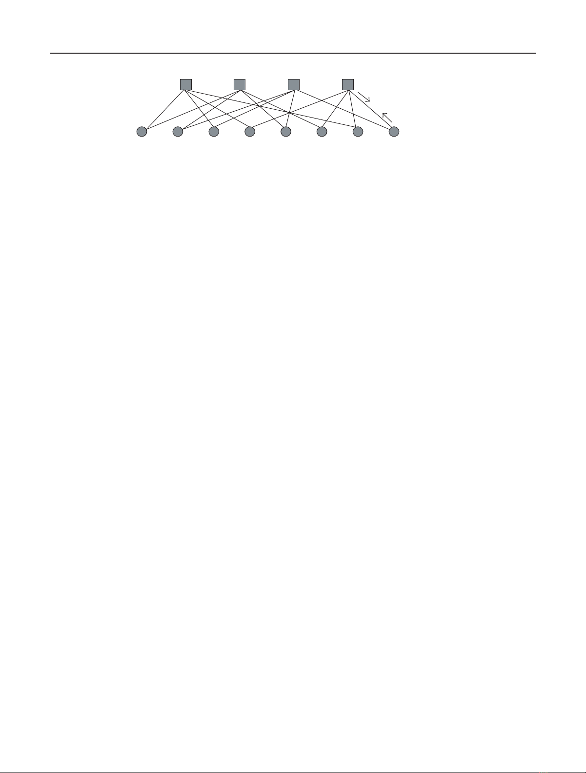
as illustrated in Figure 1, directly matches the Tanner graph:
decoding messages are iteratively computed on each variable
node and check node and exchanged through the edges be-
tween the neighboring nodes.
Recently, tremendous efforts have been devoted to ana-
lyze and improve the LDPC codes error-correcting capabil-
ity, see [4,5,6,7,8,9,10,11] and so forth. Besides their
powerful error-correcting capability, another important rea-
son why LDPC codes attract so many attention is that the
iterative BP decoding algorithm is inherently fully parallel,
thus a great potential decoding speed can be expected.
The high-speed decoder hardware implementation is ob-
viously one of the most crucial issues determining the extent
of LDPC applications in the real world. The most natural so-
lution for the decoder architecture design is to directly in-
stantiate the BP decoding algorithm to hardware: each vari-
able node and check node are physically assigned their own
processors and all the processors are connected through an
interconnection network reflecting the Tanner graph con-
nectivity. By completely exploiting the parallelism of the BP
decoding algorithm, such fully parallel decoder can achieve
very high decoding speed, for example, a 1024-bit, rate-1/2
LDPC code fully parallel decoder with the maximum symbol
throughput of 1 Gbps has been physically implemented us-
ing ASIC technology [12]. The main disadvantage of such
An FPGA Implementation of (3,6)-Regular LDPC Code Decoder 531
Check nodes
Variable nodes
Check-to-variable
message
Variable-to-check
message
Figure 1: Tanner graph representation of an LDPC code and the decoding messages flow.
fully parallel design is that with the increase of code length,
typically the LDPC code length is very large (at least several
thousands), the incurred hardware complexity will become
more and more prohibitive for many practical purposes,
for example, for 1-K code length, the ASIC decoder imple-
mentation [12]consumes1.7M gates. Moreover, as pointed
out in [12], the routing overhead for implementing the en-
tire interconnection network will become quite formidable
due to the large code length and randomness of the Tan-
ner graph. Thus high-speed partly parallel decoder de-
sign approaches that achieve appropriate trade-offsbetween
hardware complexity and decoding throughput are highly
desirable.
For any given LDPC code, due to the randomness of its
Tanner graph, it is nearly impossible to directly develop a
high-speed partly parallel decoder architecture. To circum-
vent this difficulty, Boutillon et al. [13]proposedadecoder-
first code design methodology: instead of trying to conceive
the high-speed partly parallel decoder for any given ran-
dom LDPC code, use an available high-speed partly par-
allel decoder to define a constrained random LDPC code.
We may consider it as an application of the well-known
“Think in the reverse direction” methodology. Inspired by
the decoder-first code design methodology, we proposed
ajoint code and decoder design methodology in [14]for
(3,k)-regular LDPC code partly parallel decoder design. By
jointly conceiving the code construction and partly paral-
lel decoder architecture design, we presented a (3,k)-regular
LDPC code partly parallel decoder structure in [14], which
not only defines very good (3,k)-regular LDPC codes but
also could potentially achieve high-speed partly parallel
decoding.
In this paper, applying the joint code and decoder design
methodology, we develop an elaborate (3,k)-regular LDPC
code high-speed partly parallel decoder architecture based
on which we implement a 9216-bit, rate-1/2(3,6)-regular
LDPC code decoder using Xilinx Virtex FPGA (Field Pro-
grammable Gate Array) device. In this work, we significantly
modify the original decoder structure [14] to improve the de-
coding throughput and simplify the control logic design. To
achieve good error-correcting capability, the LDPC code de-
coder architecture has to possess randomness to some extent,
which makes the FPGA implementations more challenging
since FPGA has fixed and regular hardware resources. We
propose a novel scheme to realize the random connectivity
by concatenating two routing networks, where all the ran-
dom hardwire routings are localized and the overall routing
complexity is significantly reduced. Exploiting the good min-
imum distance property of LDPC codes, this decoder em-
ploys parity check as the earlier decoding stopping criterion
to achieve adaptive decoding for energy reduction. With the
maximum 18 decoding iterations, this FPGA partly parallel
decoder supports a maximum of 54 Mbps symbol through-
put and achieves BER (bit error rate) 10−6at 2 dB over
AWGN channel.
This paper begins with a brief description of the LDPC
code decoding algorithm in Section 2.InSection 3,webriefly
describe the joint code and decoder design methodology for
(3,k)-regular LDPC code partly parallel decoder design. In
Section 4, we present the detailed high-speed partly parallel
decoder architecture design. Finally, an FPGA implementa-
tion of a (3,6)-regular LDPC code partly parallel decoder is
discussed in Section 5.
2. DECODING ALGORITHM
Since the direct implementation of BP algorithm will incur
too high hardware complexity due to the large number of
multiplications, we introduce some logarithmic quantities
to convert these complicated multiplications into additions,
which lead to the Log-BP algorithm [2,15].
Before the description of Log-BP decoding algorithm,
we introduce some definitions as follows. Let Hdenote the
M×Nsparse parity-check matrix of the LDPC code and
Hi,j denote the entry of Hat the position (i, j). We de-
fine the set of bits nthat participate in parity-check mas
ᏺ(m)={n:Hm,n =1}, and the set of parity-checks min
which bit nparticipates as ᏹ(n)={m:Hm,n =1}.Wede-
note the set ᏺ(m) with bit nexcluded by ᏺ(m)\n, and the
set ᏹ(n) with parity-check mexcluded by ᏹ(n)\m.
Algorithm 1 (Iterative Log-BP Decoding Algorithm).
Input
The prior probabilities p0
n=P(xn=0) and p1
n=P(xn=1) =
1−p0
n,n=1,...,N;
Output
Hard decision x={x1,...,xN};
Procedure
(1) Initialization: For each n, compute the intrinsic (or
channel) message γn=log p0
n/p1
nand for each (m, n)∈
532 EURASIP Journal on Applied Signal Processing
High-speed partly
parallel decoder
Random input H3
Constrained random
parameters
Construction of
H=H1
H2
Deterministic
input
H
(3,k)-regular LDPC code
ensemble defined by
H=
H
H3Selected code
Figure 2: Joint design flow diagram.
{(i, j)|Hi,j =1},compute
αm,n =sign γnlog 1+e−|γn|
1−e−|γn|,(1)
where
sign γn=
+1,γ
n≥0,
−1,γ
n<0.(2)
(2) Iterative decoding
(i) Horizontal (or check node computation) step: for
each (m, n)∈{(i, j)|Hi,j =1},compute
βm,n =log 1+e−α
1−e−α
n′∈ᏺ(m)\n
sign αm,n′,(3)
where α=n′∈ᏺ(m)\n|αm,n′|.
(ii) Vertical (or variable node computation) step: for
each (m, n)∈{(i, j)|Hi,j =1},compute
αm,n =sign γm,nlog 1+e−|γm,n|
1−e−|γm,n|,(4)
where γm,n =γn+m′∈ᏹ(n)\mβm′,n.Foreach
n, update the pseudoposterior log-likelihood ratio
(LLR) λnas
λn=γn+
m∈ᏹ(n)
βm,n.(5)
(iii) Decision step:
(a) perform hard decision on {λ1,...,λ
N}to ob-
tain x={x1,...,xN}such that xn=0if
λn>0and xn=1if λ≤0;
(b) if H·x=0, then algorithm terminates, else go
to horizontal step until the preset maximum
number of iterations have occurred.
We ca ll αm,n and βm,n in the above algorithm extrinsic
messages, where αm,n is delivered from variable node to check
node and βm,n is delivered from check node to variable node.
Each decoding iteration can be performed in fully paral-
lel fashion by physically mapping each check node to one in-
dividual check node processing unit (CNU) and each variable
node to one individual variable node processing unit (VNU).
Moreover, by delivering the hard decision xifrom each VNU
to its neighboring CNUs, the parity-check H·xcan be eas-
ily performed by all the CNUs. Thanks to the good min-
imum distance property of LDPC code, such adaptive de-
coding scheme can effectively reduce the average energy con-
sumption of the decoder without performance degradation.
In the partly parallel decoding, the operations of a cer-
tain number of check nodes or variable nodes are time-
multiplexed, or folded [16], to a single CNU or VNU. For
an LDPC code with Mcheck nodes and Nvariable nodes, if
its partly parallel decoder contains MpCNUs and NpVNUs,
we denote M/Mpas CNU folding factor and N/Npas VNU
folding factor.
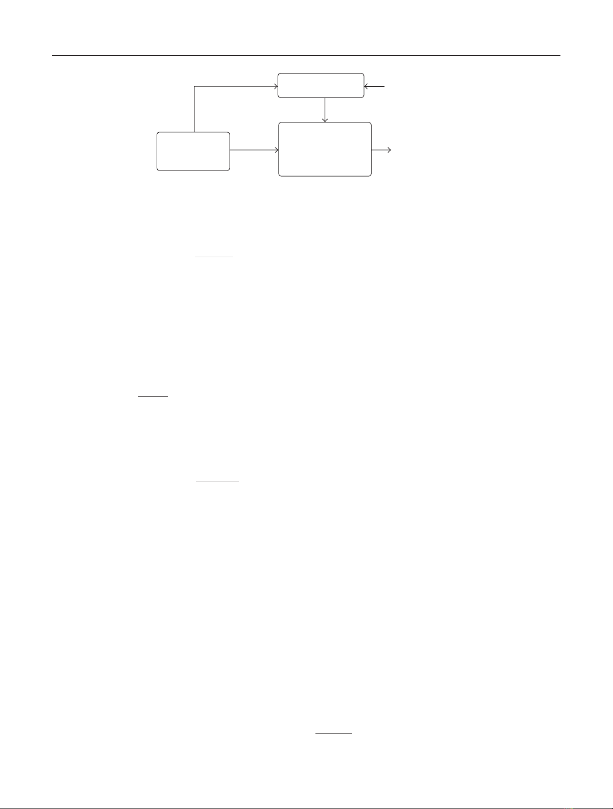
3. JOINT CODE AND DECODER DESIGN
In this section, we briefly describe the joint (3,k)-regular
LDPC code and decoder design methodology [14]. It is well
known that the BP (or Log-BP) decoding algorithm works
well if the underlying Tanner graph is 4-cycle free and does
not contain too many short cycles. Thus the motivation of
this joint design approach is to construct an LDPC code that
not only fits to a high-speed partly parallel decoder but also
has the average cycle length as large as possible in its 4-cycle-
free Tanner graph. This joint design process is outlined as fol-
lows and the corresponding schematic flow diagram is shown
in Figure 2.
(1) Explicitly construct two matrices H1and H2in such a
way that
H=[HT
1,HT
2]Tdefines a (2,k)-regular LDPC
code C2whose Tanner graph has the girth1of 12.
(2) Develop a partly parallel decoder that is configured by
a set of constrained random parameters and defines
a(3,k)-regular LDPC code ensemble, in which each
code is a subcode of C2and has the parity-check matrix
H=[
HT,HT
3]T.
(3) Select a good (3,k)-regular LDPC code from the code
ensemble based on the criteria of large Tanner graph
average cycle length and computer simulations. Typi-
cally the parity-check matrix of the selected code has
only few redundant checks, so we may assume that the
code rate is always 1 −3/k.
1Girth is the length of a shortest cycle in a graph.
An FPGA Implementation of (3,6)-Regular LDPC Code Decoder 533
H=
H1
H2=
L
I1,1
I2,1
...
Ik,1
I1,2
I2,2
...
Ik,2
00 0
···
I1,k
I2,k
...
Ik,k
000
P1,1P2,1···Pk,1
0
P1,2P2,2··· Pk,2
0
0
...
P1,k P2,k ··· Pk,k
0
L·k
L·k
N=L·k2
Figure 3: Structure of
H=[HT
1,HT
2]T.
Construction of
H=[HT
1,HT
2]T
The structure of
His shown in Figure 3, where both H1and
H2are L·kby L·k2submatrices. Each block matrix Ix,y in
H1is an L×Lidentity matrix and each block matrix Px,y
in H2is obtained by a cyclic shift of an L×Lidentity ma-
trix. Let Tdenote the right cyclic shift operator where Tu(Q)
represents right cyclic shifting matrix Qby ucolumns, then
Px,y =Tu(I)whereu=((x−1) ·y)modLand Irepresents
the L×Lidentity matrix, for example, if L=5, x=3, and
y=4, we have u=(x−1) ·ymod L=8mod5=3, then
P3,4=T3(I)=
00010
00001
10000
01000
00100
.(6)
Notice that in both H1and H2, each row contains k1’s
and each column contains a single 1. Thus, the matrix
H=
[HT
1,HT
2]Tdefines a (2,k)-regular LDPC code C2with L·
k2variable nodes and 2L·kcheck nodes. Let Gdenote the
Tanner graph of C2, we have the following theorem regarding
to the girth of G.
Theorem 1. If Lcannot be factored as L=a·b,wherea, b ∈
{0,...,k−1}, then the girth of Gis 12 and there is at least one
12-cycle passing each check node.
Partly parallel decoder
Based on the specific structure of
H, a principal (3,k)-regular
LDPC code partly parallel decoder structure was presented in
[14]. This decoder is configured by a set of constrained ran-
dom parameters and defines a (3,k)-regular LDPC code en-
semble. Each code in this ensemble is essentially constructed
by inserting extra L·kcheck nodes to the high-girth (2,k)-
regular LDPC code C2under the constraint specified by the
decoder. Therefore, it is reasonable to expect that the codes
in this ensemble more likely do not contain too many short
cycles and we may easily select a good code from it. For real
applications, we can select a good code from this code ensem-
ble as follows: first in the code ensemble, find several codes
with relatively high-average cycle lengths, then select the one
leading to the best result in the computer simulations.
The principal partly parallel decoder structure presented
in [14] has the following properties.
(i) It contains k2memory banks, each one consists of sev-
eral RAMs to store all the decoding messages associ-
ated with Lvariable nodes.
(ii) Each memory bank associates with one address gener-
ator that is configured by one element in a constrained
random integer set .
(iii) It contains a configurable random-like one-dimen-
sional shufflenetworkwith the routing complexity
scaled by k2.
(iv) It contains k2VNUs and kCNUs so that the VNU and
CNU folding factors are L·k2/k2=Land 3L·k/k =3L,
respectively.
(v) Each iteration completes in 3Lclock cycles in which
only CNUs work in the first 2Lclock cycles and both
CNUs and VNUs work in the last Lclock cycles.
Over all the possible and , this decoder defines a (3,k)-
regular LDPC code ensemble in which each code has the
parity-check matrix H=[
HT,HT
3]T, where the submatrix
H3is jointly specified by and S.
4. PARTLY PARALLEL DECODER ARCHITECTURE
In this paper, applying the joint code and decoder design
methodology, we develop a high-speed (3,k)-regular LDPC
code partly parallel decoder architecture based on which a
9216-bit, rate-1/2(3,6)-regular LDPC code partly parallel
decoder has been implemented using Xilinx Virtex FPGA
device. Compared with the structure presented in [14], this
partly parallel decoder architecture has the following distinct
characteristics.
(i) It employs a novel concatenated configurable ran-
dom two-dimensional shuffle network implementa-
tion scheme to realize the random-like connectivity
with low routing overhead, which is especially desir-
able for FPGA implementations.
(ii) To improve the decoding throughput, both the VNU
folding factor and CNU folding factor are Linstead of
Land 3Lin the structure presented in [14].
(iii) To simplify the control logic design and reduce the
memory bandwidth requirement, this decoder com-
pletes each decoding iteration in 2Lclock cycles in
which CNUs and VNUs work in the 1st and 2nd L
clock cycles, alternatively.
Following the joint design methodology, we have that this
decoder should define a (3,k)-regular LDPC code ensemble
in which each code has L·k2variable nodes and 3L·kcheck
nodes and, as illustrated in Figure 4, the parity-check ma-
trix of each code has the form H=[HT
1,HT
2,HT
3]Twhere H1
and H2have the explicit structures as shown in Figure 3 and
the random-like H3is specified by certain configuration pa-
rameters of the decoder. To facilitate the description of the

534 EURASIP Journal on Applied Signal Processing
H=
H1
H2
H3
=
Leftmost column
Lh(k,2)
1
Rightmost column
h(k,2)
L
I1,1
...
Ik,1
I1,2
...
Ik,2
···
I1,k ...
Ik,k
L·k
P1,1··· Pk,1
P1,2··· Pk,2
...
P1,k ··· Pk,k
L·k
L·k
H(k,2) L·k2
Figure 4: The parity-check matrix.
decoder architecture, we introduce some definitions as fol-
lows: we denote the submatrix consisting of the Lconsecutive
columns in Hthat go through the block matrix Ix,y as H(x,y)
in which, from left to right, each column is labeled as h(x,y)
i
with iincreasing from 1 to L, as shown in Figure 4.Welabel
the variable node corresponding to column h(x,y)
ias v(x,y)
iand
the Lvariable nodes v(x,y)
ifor i=1,...,Lconstitute a variable
node group VGx,y. Finally, we arrange the L·kcheck nodes
corresponding to all the L·krows of submatrix Hiinto check
node group CGi.
Figure 5 shows the principal structure of this partly par-
allel decoder. It mainly contains k2PE blocks PEx,y,for1≤x
and y≤k, three bidirectional shufflenetworksπ1,π2,and
π3,and3·kCNUs. Each PEx,y contains one memory bank
RAMsx,y that stores all the decoding messages, including the
intrinsic and extrinsic messages and hard decisions, associ-
ated with all the Lvariable nodes in the variable node group
VGx,y, and contains one VNU to perform the variable node
computations for these Lvariable nodes. Each bidirectional
shufflenetworkπirealizes the extrinsic message exchange be-
tween all the L·k2variable nodes and the L·kcheck nodes in
CGi.ThekCNUi, j ,for j=1,...,k, perform the check node
computations for all the L·kcheck nodes in CGi.
This decoder completes each decoding iteration in 2L
clock cycles, and during the first and second Lclock cycles,
it works in check node processing mode and variable node
processing mode, respectively. In the check node processing
mode, the decoder not only performs the computations of
all the check nodes but also completes the extrinsic message
exchange between neighboring nodes. In variable node pro-
cessing mode, the decoder only performs the computations
of all the variable nodes.
The intrinsic and extrinsic messages are all quantized to
five bits and the iterative decoding datapaths of this partly
parallel decoder are illustrated in Figure 6, in which the dat-
apaths in check node processing and variable node process-
ing are represented by solid lines and dash dot lines, respec-
tively. As shown in Figure 6,eachPEblockPE
x,y contains
five RAM blocks: EXT RAM ifor i=1,2,3, INT RAM, and
DEC RAM. Each EXT RAM ihas Lmemory locations and
the location with the address d−1(1≤d≤L) contains
the extrinsic messages exchanged between the variable node
v(x,y)
din VGx,y and its neighboring check node in CGi.The
INT RAM and DEC RAM store the intrinsic message and
hard decision associated with node v(x,y)
dat the memory lo-
cation with the address d−1(1≤d≤L). As we will see
later, such decoding messages storage strategy could greatly
simplify the control logic for generating the memory access
address.
For the purpose of simplicity, in Figure 6 we do not show
the datapath from INT RAM to EXT RAM i’s for extrinsic
message initialization, which can be easily realized in Lclock
cycles before the decoder enters the iterative decoding pro-
cess.
4.1. Check node processing
During the check node processing, the decoder performs the
computations of all the check nodes and realizes the extrinsic
message exchange between all the neighboring nodes. At the
beginning of check node processing, in each PEx,y the mem-
ory location with address d−1inEXTRAM icontains 6-
bit hybrid data that consists of 1-bit hard decision and 5-bit
variable-to-check extrinsic message associated with the vari-
able node v(x,y)
din VGx,y. In each clock cycle, this decoder
performs the read-shuffle-modify-unshuffle-write operations
to convert one variable-to-check extrinsic message in each
EXT RAM ito its check-to-variable counterpart. As illus-
trated in Figure 6, we may outline the datapath loop in check
node processing as follows:
(1) read:one6-bithybriddatah(i)
x,y is read from each
EXT RAM iin each PEx,y;
(2) shuffle:eachhybriddatah(i)
x,y goes through the shuffle
network πiand arrives at CNUi, j ;
(3) modify:eachCNU
i,j performs the parity check on the 6
input hard decision bits and generates the 6 output 5-
bit check-to-variable extrinsic messages β(i)
x,y based on
the 6 input 5-bit variable-to-check extrinsic messages;
(4) unshuffle: send each check-to-variable extrinsic mes-
sage β(i)
x,y back to the PE block via the same path as its
variable-to-check counterpart;
(5) write:writeeachβ(i)
x,y to the same memory location in
EXT RAM ias its variable-to-check counterpart.
All the CNUs deliver the parity-check results to a central
control block that will, at the end of check node processing,
determine whether all the parity-check equations specified
by the parity-check matrix have been satisfied, if yes, the de-
coding for current code frame will terminate.
To achieve higher decoding throughput, we implement
the read-shuffle-modify-unshuffle-write loop operation by
five-stage pipelining as shown in Figure 7, where CNU is
one-stage pipelined. To make this pipelining scheme feasi-
ble, we realize each bidirectional I/O connection in the three

![Thuyết minh tính toán kết cấu đồ án Bê tông cốt thép 1: [Mô tả/Hướng dẫn/Chi tiết]](https://cdn.tailieu.vn/images/document/thumbnail/2016/20160531/quoccuong1992/135x160/1628195322.jpg)