SLLS047L − FEBRUARY 1989 − REVISED MARCH 2004
1
POST OFFICE BOX 655303 • DALLAS, TEXAS 75265
DMeets or Exceeds TIA/EIA-232-F and ITU
Recommendation V.28
DOperates From a Single 5-V Power Supply
With 1.0-mF Charge-Pump Capacitors
DOperates Up To 120 kbit/s
DTwo Drivers and Two Receivers
D±30-V Input Levels
DLow Supply Current ...8 mA Typical
DESD Protection Exceeds JESD 22
− 2000-V Human-Body Model (A114-A)
DUpgrade With Improved ESD (15-kV HBM)
and 0.1-mF Charge-Pump Capacitors is
Available With the MAX202
DApplications
− TIA/EIA-232-F, Battery-Powered Systems,
Terminals, Modems, and Computers
description/ordering information
The MAX232 is a dual driver/receiver that includes a capacitive voltage generator to supply TIA/EIA-232-F
voltage levels from a single 5-V supply. Each receiver converts TIA/EIA-232-F inputs to 5-V TTL/CMOS levels.
These receivers have a typical threshold of 1.3 V, a typical hysteresis of 0.5 V, and can accept ±30-V inputs.
Each driver converts TTL/CMOS input levels into TIA/EIA-232-F levels. The driver, receiver, and
voltage-generator functions are available as cells in the Texas Instruments LinASIC library.
ORDERING INFORMATION
TAPACKAGE†ORDERABLE
PART NUMBER
TOP-SIDE
MARKING
PDIP (N) Tube of 25 MAX232N MAX232N
SOIC (D)
Tube of 40 MAX232D
MAX232
0°C to 70°C
SOIC (D) Reel of 2500 MAX232DR MAX232
0°C to 70°C
SOIC (DW)
Tube of 40 MAX232DW
MAX232
SOIC (DW) Reel of 2000 MAX232DWR MAX232
SOP (NS) Reel of 2000 MAX232NSR MAX232
PDIP (N) Tube of 25 MAX232IN MAX232IN
SOIC (D)
Tube of 40 MAX232ID
MAX232I
−40°C to 85°CSOIC (D) Reel of 2500 MAX232IDR MAX232I
−40 C to 85 C
SOIC (DW)
Tube of 40 MAX232IDW
MAX232I
SOIC (DW)
Reel of 2000 MAX232IDWR
MAX232I
†Package drawings, standard packing quantities, thermal data, symbolization, and PCB design
guidelines are available at www.ti.com/sc/package.
Copyright 2004, Texas Instruments Incorporated
!"# $"%&! '#(
'"! ! $#!! $# )# # #* "#
'' +,( '"! $!#- '# #!#&, !&"'#
#- && $##(
Please be aware that an important notice concerning availability, standard warranty, and use in critical applications of
Texas Instruments semiconductor products and disclaimers thereto appears at the end of this data sheet.
LinASIC is a trademark of Texas Instruments.
1
2
3
4
5
6
7
8
16
15
14
13
12
11
10
9
C1+
VS+
C1−
C2+
C2−
VS−
T2OUT
R2IN
VCC
GND
T1OUT
R1IN
R1OUT
T1IN
T2IN
R2OUT
MAX232 . . . D, DW, N, OR NS PACKAGE
MAX232I . . . D, DW, OR N PACKAGE
(TOP VIEW)
SLLS047L − FEBRUARY 1989 − REVISED MARCH 2004
2POST OFFICE BOX 655303 • DALLAS, TEXAS 75265
Function Tables
EACH DRIVER
INPUT
TIN
OUTPUT
TOUT
L H
H L
H = high level, L = low
level
EACH RECEIVER
INPUT
RIN
OUTPUT
ROUT
L H
H L
H = high level, L = low
level
logic diagram (positive logic)
T1IN T1OUT
R1INR1OUT
T2IN T2OUT
R2INR2OUT
11
10
12
9
14
7
13
8
SLLS047L − FEBRUARY 1989 − REVISED MARCH 2004
3
POST OFFICE BOX 655303 • DALLAS, TEXAS 75265
absolute maximum ratings over operating free-air temperature range (unless otherwise noted)†
Input supply voltage range, VCC (see Note 1) −0.3 V to 6 V. . . . . . . . . . . . . . . . . . . . . . . . . . . . . . . . . . . . . . . . . .
Positive output supply voltage range, VS+ V
CC − 0.3 V to 15 V. . . . . . . . . . . . . . . . . . . . . . . . . . . . . . . . . . . . . . .
Negative output supply voltage range, VS− −0.3 V to −15 V. . . . . . . . . . . . . . . . . . . . . . . . . . . . . . . . . . . . . . . . . .
Input voltage range, VI: Driver −0.3 V to VCC + 0.3 V. . . . . . . . . . . . . . . . . . . . . . . . . . . . . . . . . . . . . . . . . . . . . . . .
Receiver ±30 V. . . . . . . . . . . . . . . . . . . . . . . . . . . . . . . . . . . . . . . . . . . . . . . . . . . . . . . . . . .
Output voltage range, VO: T1OUT, T2OUT VS− − 0.3 V to VS+ + 0.3 V. . . . . . . . . . . . . . . . . . . . . . . . . . . . . . . .
R1OUT, R2OUT −0.3 V to VCC + 0.3 V. . . . . . . . . . . . . . . . . . . . . . . . . . . . . . . . . . . .
Short-circuit duration: T1OUT, T2OUT Unlimited. . . . . . . . . . . . . . . . . . . . . . . . . . . . . . . . . . . . . . . . . . . . . . . . . . .
Package thermal impedance, θJA (see Notes 2 and 3): D package 73°C/W. . . . . . . . . . . . . . . . . . . . . . . . . . . .
DW package 57°C/W. . . . . . . . . . . . . . . . . . . . . . . . . .
N package 67°C/W. . . . . . . . . . . . . . . . . . . . . . . . . . . .
NS package 64°C/W. . . . . . . . . . . . . . . . . . . . . . . . . . .
Operating virtual junction temperature, TJ 150°C. . . . . . . . . . . . . . . . . . . . . . . . . . . . . . . . . . . . . . . . . . . . . . . . . . .
Storage temperature range, Tstg −65°C to 150°C. . . . . . . . . . . . . . . . . . . . . . . . . . . . . . . . . . . . . . . . . . . . . . . . . .
†Stresses beyond those listed under “absolute maximum ratings” may cause permanent damage to the device. These are stress ratings only, and
functional operation of the device at these or any other conditions beyond those indicated under “recommended operating conditions” is not
implied. Exposure to absolute-maximum-rated conditions for extended periods may affect device reliability.
NOTES: 1. All voltages are with respect to network GND.
2. Maximum power dissipation is a function of TJ(max), θJA, and TA. The maximum allowable power dissipation at any allowable
ambient temperature is PD = (TJ(max) − TA)/θJA. Operating at the absolute maximum TJ of 150°C can affect reliability.
3. The package thermal impedance is calculated in accordance with JESD 51-7.
recommended operating conditions
MIN NOM MAX UNIT
VCC Supply voltage 4.5 5 5.5 V
VIH High-level input voltage (T1IN,T2IN) 2 V
VIL Low-level input voltage (T1IN, T2IN) 0.8 V
R1IN, R2IN Receiver input voltage ±30 V
TA
Operating free-air temperature
MAX232 0 70
°C
T
A
Operating free-air temperature
MAX232I −40 85 °
C
electrical characteristics over recommended ranges of supply voltage and operating free-air
temperature (unless otherwise noted) (see Note 4 and Figure 4)
PARAMETER TEST CONDITIONS MIN TYP‡MAX UNIT
ICC Supply current VCC = 5.5 V,
TA = 25°C
All outputs open, 8 10 mA
‡All typical values are at VCC = 5 V and TA = 25°C.
NOTE 4: Test conditions are C1−C4 = 1 µF at VCC = 5 V ±0.5 V.
SLLS047L − FEBRUARY 1989 − REVISED MARCH 2004
4POST OFFICE BOX 655303 • DALLAS, TEXAS 75265
DRIVER SECTION
electrical characteristics over recommended ranges of supply voltage and operating free-air
temperature range (see Note 4)
PARAMETER TEST CONDITIONS MIN TYP†MAX UNIT
VOH High-level output voltage T1OUT, T2OUT RL = 3 kΩ to GND 5 7 V
VOL Low-level output voltage‡T1OUT, T2OUT RL = 3 kΩ to GND −7 −5 V
roOutput resistance T1OUT, T2OUT VS+ = VS− = 0, VO = ±2 V 300 Ω
IOS§Short-circuit output current T1OUT, T2OUT VCC = 5.5 V, VO = 0 ±10 mA
IIS Short-circuit input current T1IN, T2IN VI = 0 200 µA
†All typical values are at VCC = 5 V, TA = 25°C.
‡The algebraic convention, in which the least-positive (most negative) value is designated minimum, is used in this data sheet for logic voltage
levels only.
§Not more than one output should be shorted at a time.
NOTE 4: Test conditions are C1−C4 = 1 µF at VCC = 5 V ±0.5 V.
switching characteristics, VCC = 5 V, TA = 25°C (see Note 4)
PARAMETER TEST CONDITIONS MIN TYP MAX UNIT
SR Driver slew rate RL = 3 kΩ to 7 kΩ,
See Figure 2 30 V/µs
SR(t) Driver transition region slew rate See Figure 3 3 V/µs
Data rate One TOUT switching 120 kbit/s
NOTE 4: Test conditions are C1−C4 = 1 µF at VCC = 5 V ±0.5 V.
RECEIVER SECTION
electrical characteristics over recommended ranges of supply voltage and operating free-air
temperature range (see Note 4)
PARAMETER TEST CONDITIONS MIN TYP†MAX UNIT
VOH High-level output voltage R1OUT, R2OUT IOH = −1 mA 3.5 V
VOL Low-level output voltage‡R1OUT, R2OUT IOL = 3.2 mA 0.4 V
VIT+ Receiver positive-going input
threshold voltage R1IN, R2IN VCC = 5 V, TA = 25°C 1.7 2.4 V
VIT− Receiver negative-going input
threshold voltage R1IN, R2IN VCC = 5 V, TA = 25°C 0.8 1.2 V
Vhys Input hysteresis voltage R1IN, R2IN VCC = 5 V 0.2 0.5 1 V
riReceiver input resistance R1IN, R2IN VCC = 5, TA = 25°C 3 5 7 kΩ
†All typical values are at VCC = 5 V, TA = 25°C.
‡The algebraic convention, in which the least-positive (most negative) value is designated minimum, is used in this data sheet for logic voltage
levels only.
NOTE 4: Test conditions are C1−C4 = 1 µF at VCC = 5 V ±0.5 V.
switching characteristics, VCC = 5 V, TA = 25°C (see Note 4 and Figure 1)
PARAMETER TYP UNIT
tPLH(R) Receiver propagation delay time, low- to high-level output 500 ns
tPHL(R) Receiver propagation delay time, high- to low-level output 500 ns
NOTE 4: Test conditions are C1−C4 = 1 µF at VCC = 5 V ±0.5 V.
SLLS047L − FEBRUARY 1989 − REVISED MARCH 2004
5
POST OFFICE BOX 655303 • DALLAS, TEXAS 75265
PARAMETER MEASUREMENT INFORMATION
≤10 ns
VCC
R1IN
or
R2IN
R1OUT
or
R2OUT
RL = 1.3 kΩ
See Note C
CL = 50 pF
(see Note B)
TEST CIRCUIT
≤10 ns
Input
Output
tPHL tPLH
1.5 V VOL
VOH
0 V
3 V
10%
90%
50%
500 ns
WAVEFORMS
1.5 V
90%
50% 10%
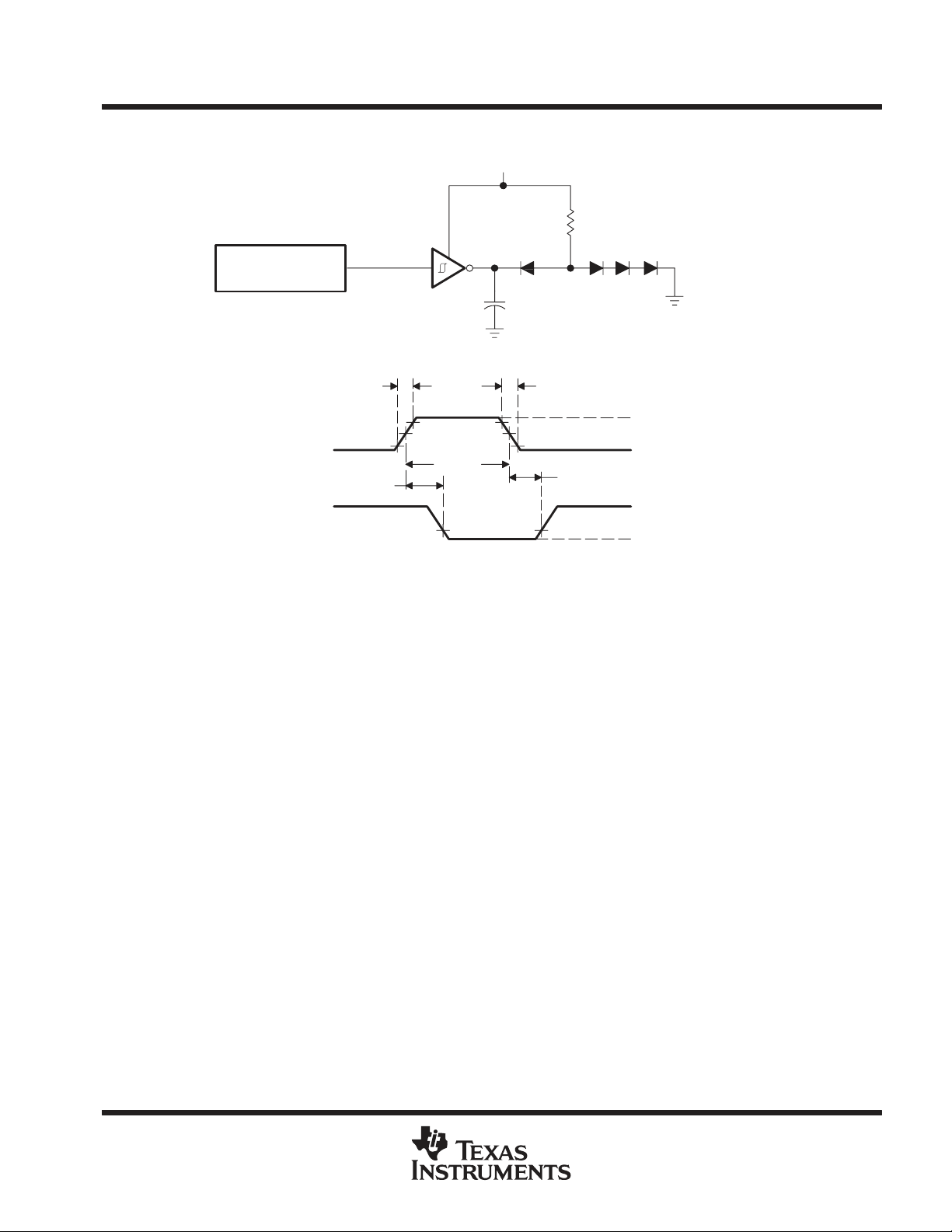
NOTES: A. The pulse generator has the following characteristics: ZO = 50 Ω, duty cycle ≤ 50%.
B. CL includes probe and jig capacitance.
C. All diodes are 1N3064 or equivalent.
Pulse
Generator
(see Note A)
Figure 1. Receiver Test Circuit and Waveforms for tPHL and tPLH Measurements
![Cắt bằng hồ quang điện [Mới Nhất]](https://cdn.tailieu.vn/images/document/thumbnail/2014/20140331/hoangtuxuquang/135x160/7351396310863.jpg)


![Thanh ghi: Chương 8 [Hướng dẫn chi tiết]](https://cdn.tailieu.vn/images/document/thumbnail/2011/20110508/thanhmaikmt/135x160/chuong_8_thanh_ghi_1565.jpg)


%20--%3e%3cdefs%3e%3cstyle%3e%20.st0%20{%20fill:%20%23fff;%20}%20.st1%20{%20fill:%20%237800fa;%20}%20%3c/style%3e%3c/defs%3e%3cpath%20class='st1'%20d='M117.78,12.18H43.11c2.9,3.47,4.65,7.94,4.65,12.82,0,5.6-2.3,10.66-6.01,14.29h76.02l7.22-13.56-7.22-13.56Z'/%3e%3cg%3e%3cpath%20class='st0'%20d='M53.58,26.17h-.59v-1.46h.59v-4.96h2.83c1.78,0,2.67.94,2.67,2.82v5.76c0,1.87-.89,2.81-2.67,2.81h-2.83v-4.96ZM55.36,21.37v3.34h1.1v1.46h-1.1v3.34h1.01c.61,0,.91-.37.91-1.1v-5.93c0-.74-.3-1.1-.91-1.1h-1.01Z'/%3e%3cpath%20class='st0'%20d='M65.99,31.14h-1.8l-.31-2.07h-2.19l-.31,2.07h-1.64l1.82-11.39h2.62l1.82,11.39ZM65.28,18.04c-.25.46-.51.77-.75.94-.21.15-.47.22-.79.22-.26,0-.57-.07-.92-.22l-.38-.15c-.14-.05-.26-.07-.37-.07-.3,0-.53.18-.71.54l-.91-.68c.25-.46.51-.77.75-.94.21-.14.48-.21.79-.21.26,0,.57.07.92.21l.38.15c.14.05.26.07.37.07.3,0,.53-.18.71-.54l.91.68ZM61.91,27.52h1.73l-.87-5.76-.87,5.76Z'/%3e%3cpath%20class='st0'%20d='M74.53,26.89v1.52c0,1.91-.89,2.86-2.67,2.86s-2.67-.95-2.67-2.86v-5.93c0-1.91.89-2.86,2.67-2.86s2.67.95,2.67,2.86v1.11h-1.69v-1.22c0-.75-.31-1.12-.93-1.12s-.93.37-.93,1.12v6.15c0,.74.31,1.11.93,1.11s.93-.37.93-1.11v-1.63h1.69Z'/%3e%3cpath%20class='st0'%20d='M81.4,31.14h-1.8l-.31-2.07h-2.19l-.31,2.07h-1.64l1.82-11.39h2.62l1.82,11.39ZM75.9,19.2l1.52-1.91h1.71l1.51,1.91h-1.61l-.76-.95-.75.95h-1.61ZM77.32,27.52h1.73l-.87-5.76-.87,5.76ZM83.1,15.99l-1.76,1.91h-1.26l1.17-1.91h1.86Z'/%3e%3cpath%20class='st0'%20d='M84.86,19.75c1.78,0,2.67.94,2.67,2.82v1.48c0,1.87-.89,2.81-2.67,2.81h-.85v4.28h-1.79v-11.39h2.64ZM84.01,21.37v3.86h.85c.58,0,.87-.36.87-1.08v-1.71c0-.71-.29-1.07-.87-1.07h-.85Z'/%3e%3cpath%20class='st0'%20d='M93.51,19.75c1.78,0,2.67.94,2.67,2.82v1.48c0,1.87-.89,2.81-2.67,2.81h-.85v4.28h-1.79v-11.39h2.64ZM92.66,21.37v3.86h.85c.58,0,.87-.36.87-1.08v-1.71c0-.71-.29-1.07-.87-1.07h-.85Z'/%3e%3cpath%20class='st0'%20d='M98.8,31.14h-1.79v-11.39h1.79v4.88h2.03v-4.88h1.83v11.39h-1.83v-4.88h-2.03v4.88Z'/%3e%3cpath%20class='st0'%20d='M105.36,24.55h2.46v1.62h-2.46v3.34h3.09v1.63h-4.88v-11.39h4.88v1.63h-3.09v3.18ZM108.17,17.29l-1.76,1.91h-1.26l1.17-1.91h1.86Z'/%3e%3cpath%20class='st0'%20d='M112.2,19.75c1.78,0,2.67.94,2.67,2.82v1.48c0,1.87-.89,2.81-2.67,2.81h-.85v4.28h-1.79v-11.39h2.64ZM111.35,21.37v3.86h.85c.58,0,.87-.36.87-1.08v-1.71c0-.71-.29-1.07-.87-1.07h-.85Z'/%3e%3c/g%3e%3ccircle%20class='st1'%20cx='25'%20cy='25'%20r='20'/%3e%3cpath%20class='st0'%20d='M32.78,19.27c2.92,0,4.43,2.55,5.28,5.33l.71,2.17c.14.38-.33.75-.71.75h-5.61c.19-.33.24-.71.09-1.08l-.75-2.45c-.43-1.32-.99-2.64-1.79-3.77.75-.57,1.65-.94,2.78-.94h0ZM25,18.38c3.25,0,4.9,2.78,5.89,5.89l.76,2.45c.14.42-.33.8-.8.8h-11.69c-.42,0-.94-.38-.8-.8l.75-2.45c.99-3.11,2.64-5.89,5.89-5.89h0ZM25,11.35c1.74,0,3.11,1.37,3.11,3.11s-1.37,3.11-3.11,3.11-3.11-1.41-3.11-3.11,1.41-3.11,3.11-3.11h0ZM17.27,19.27c1.08,0,1.98.38,2.73.94-.8,1.13-1.37,2.45-1.74,3.77l-.8,2.45c-.14.38-.05.75.09,1.08h-5.56c-.42,0-.9-.38-.75-.75l.71-2.17c.9-2.78,2.41-5.33,5.33-5.33h0ZM17.27,12.91c1.51,0,2.78,1.27,2.78,2.83s-1.27,2.83-2.78,2.83-2.83-1.27-2.83-2.83,1.27-2.83,2.83-2.83h0ZM32.78,12.91c1.56,0,2.78,1.27,2.78,2.83s-1.23,2.83-2.78,2.83-2.83-1.27-2.83-2.83,1.27-2.83,2.83-2.83h0ZM27.07,28.56v.09c0,.57-.24,1.08-.61,1.46h0v.05c-.38.33-.9.57-1.46.57s-1.08-.24-1.46-.61h0c-.38-.38-.61-.9-.61-1.46v-.09h1.41v.09c0,.19.05.38.19.47v.05c.09.09.28.19.47.19s.38-.09.47-.19v-.05c.14-.09.24-.28.24-.47t-.05-.09h1.41ZM30.99,28.56v.09c0,1.65-.66,3.16-1.74,4.24-1.08,1.08-2.59,1.79-4.24,1.79s-3.16-.71-4.24-1.79l-.05-.05c-1.04-1.08-1.7-2.55-1.7-4.2v-.09h1.41v.09c0,1.27.47,2.4,1.27,3.25h.05c.85.85,1.98,1.37,3.25,1.37s2.4-.52,3.25-1.37c.85-.8,1.37-1.98,1.37-3.25v-.09h1.37ZM34.99,28.56v.09c0,2.78-1.13,5.28-2.92,7.07-1.79,1.79-4.29,2.92-7.07,2.92s-5.23-1.13-7.07-2.92c-1.79-1.79-2.92-4.29-2.92-7.07v-.09h1.41v.09c0,2.4.94,4.53,2.5,6.08,1.56,1.56,3.72,2.5,6.08,2.5s4.52-.94,6.08-2.5c1.56-1.56,2.5-3.68,2.5-6.08v-.09h1.41Z'/%3e%3c/svg%3e)