Etching techniques
-
Lecture ECE 6450 Microelectronic - Chapter 11: Etching techniques. After studying this section will help you understand Anisotropy can depend on mean Increasing Mean Free Path free path, or on DC plasma bias. Increasing mean free path (generally) increases anisotropy. Increasing DC bias (generally) increases anisotropy.
 12p
12p  trollhunters
 10-01-2022
 12
12
 0
0
 Download
-
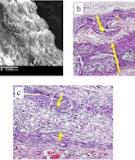
In this work a technique of metallizing substrate via electroless plating using moisture-cured polyurethane (MCPU) system as the undercoat is presented. MCPU prepolymer was prepared by mixing polyethylene glycol divinyl ether and diphenylmethane-4, 4’-diisocyanate in 1:1 ratio. The effects of etching time as well as curing period on the surface characteristic of MCPU undercoating were investigated. Contact angle measurements, FTIR and SEM were employed to study the changes on the surface of the treated MCPU undercoats prior to electroless nickel plating.
 13p
13p  12120609
 01-06-2020
 6
6
 0
0
 Download
-
In this paper we present a new fabrication technique that only uses conventional techniques of microtechnology such as microlithography, thin-film deposition and directional ion beam etching to makevery narrow, wafer-scale length platinum (Pt) nanowires, named deposition and etching under angles (DEA). Then fabricated Pt nanowires electrodes were modified by using several chemicals to immobilize glucose oxidase (GOD) enzyme for application in glucose detection. A cyclic voltammetry (CV) technique was used to determine glucose concentrations.
 11p
11p  queencongchua3
 09-09-2019
 15
15
 1
1
 Download
-
This work presents a new technique for discriminating between alpha particles of different energy levels. In a first study, two groups of alpha particles emitted from radium-226 and americium-241 sources were successfully separated using a CR-39 microfilm of appropriate thickness. This thickness was adjusted by chemical etching before and after irradiation so that lower-energy particles were stopped within the detector, while higher-energy particles were revealed on the back side of the detector.
 5p
5p  minhxaminhyeu4
 26-06-2019
 14
14
 1
1
 Download
-
Your destiny is not predetermined nor etched in stone. It is not predictable or inevitable. It is not governed by fate or providence. Your life is in your hands and you determine the life you are living now and the life you will live in the future. By knowing this, accepting it as the truth and then learning the techniques and teachings in "Living More Life" you will make it the best life you can ever live.
 110p
110p  namde04
 03-05-2013
 73
73
 15
15
 Download
-
Personal scale PCB milling machines use one of two processes, a mechanical etching process, or a process in which conductive materials are sprayed onto a base board. The mechanical etching process on a desktop circuit maker involves a rotating milling bit that mechanically etches out the desired circuit design onto a copper circuit board. Both etching and spraying techniques enable users to create multi-layer and finely detailed PCBs.
 0p
0p  quynho77
 13-11-2012
 43
43
 1
1
 Download
-
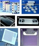
Almost all technologies described so far are suitable for prototyping or for small series production only. It simply takes a lot of time and is therefore costly to manufacture a large number of microstructures by laser ablation or wire erosion and by milling or SLM. This is not so in the case of the etching techniques. Here, a large number of microstructure devices can be very easily generated. Another possibility to obtain a large number of microstructures is by embossing.
 8p
8p  quynho77
 13-11-2012
 40
40
 1
1
 Download
-
Not all materials can be etched in an easy and cheap way. Especially, noble metals or tantalum are stable against most of these corrosive structuring methods. Hence, precision machining may be used to generate microstructures from these metals as well as from standard metal alloys such as stainless steel or hastelloy. Depending on the material, precision machining can be performed by spark erosion (wire spark erosion and countersunk spark erosion), laser machining or mechanical precision machining.
 8p
8p  quynho77
 13-11-2012
 53
53
 1
1
 Download
-
When etching techniques are used, two main considerations have to be given. First, the aspect ratio (the ratio between the width and depth of a structure), for wet chemical etching, can only be
 18p
18p  quynho77
 13-11-2012
 34
34
 1
1
 Download
-
Dry andwet etching techniques based onsiliconand other semiconductor technologies are well known. For many metals, etching is a relatively cheap and well-established technique to obtain freeform structures with dimensions in the submillimeter range. This technique iswelldescribedinthe literature[1–5,7].Aphotosensitivepolymermask material is applied on themetal to be etched. Themask is exposed to light via a primary maskwithstructural layers.Here,different technologiesare applicable, andtheirdetails canbefoundintheliteratureonsemiconductorprocessingor inRefs[1–3].
 6p
6p  quynho77
 13-11-2012
 32
32
 0
0
 Download
-
Several techniques for fabrication of through-wafer vias in silicon have been compared in terms of achievable via diameter, shape and geometry and their influence on mechanical strength of silicon dies/wafers. Assessed techniques are: powder blasting, laser melt cutting, laser ablation, and deep reactive ion etching. The resolution of each method and influence on geometry was evaluated by fabrication through-wafer holes and slots in 240µm-thick silicon wafers. The mechanical strength is measured using ring-on-ring (RoR) and four-point bending methods.
 17p
17p  quynho77
 13-11-2012
 34
34
 0
0
 Download
-
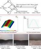
Polymer micromolding is a common way to ma microchannels, because of the ease of processing, low co and bio-compatibility. Molds with micron-scale featur may be made from photosensitive polymers (e.g., SU-8) by DRIE silicon micromachining. Poly(dimethylsiloxan (PDMS) is often chosen as the microstructural materi [15]. PDMS is spin cast onto the mold, cured and peel off. A short exposure in an oxygen plasma activates t PDMS surface and results in instant bonding to oth PDMS or glass surfaces.
 11p
11p  quynho77
 13-11-2012
 60
60
 1
1
 Download


